
Texas Instruments
CD4007UBF3A
Specialty Logic ICs


.png?x-oss-process=image/format,webp/resize,p_30)


CD4007UBF3A Description
CD4007UBF3A Description
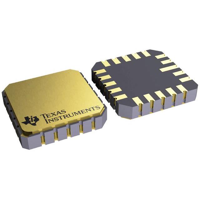
The CD4007UBF3A is a CMOS Dual Complementary Pair Plus Inverter, part of the 4000B series, manufactured by Texas Instruments. This logic IC chip is designed for versatile digital applications requiring a combination of complementary pairs and an inverter in a single package. The CD4007UBF3A is housed in a through-hole package, making it suitable for a wide range of printed circuit board (PCB) designs, including those that require robust mechanical stability and ease of manual or automated assembly. The device operates within a supply voltage range of 3V to 18V, offering flexibility in power supply requirements and compatibility with various voltage levels commonly used in digital systems.
CD4007UBF3A Features
- Logic Type: The CD4007UBF3A features a complementary pair plus inverter logic type, which allows for efficient and versatile digital signal processing. This configuration is ideal for applications requiring both N-channel and P-channel MOSFETs along with an inverter, reducing the need for multiple discrete components.
- Supply Voltage Range: With a wide operating voltage range of 3V to 18V, the CD4007UBF3A can be used in systems with varying power supply specifications, enhancing its adaptability across different electronic designs.
- Through-Hole Mounting: The through-hole package ensures secure mechanical attachment to the PCB, which is particularly beneficial in environments where vibration or mechanical stress may be a concern.
- Compliance and Standards: The CD4007UBF3A is ROHS3 compliant, adhering to stringent environmental regulations and ensuring that it is free from hazardous substances. Additionally, it is classified under ECCN EAR99 and HTSUS 8542.39.0001, facilitating international trade and regulatory compliance.
- Moisture Sensitivity Level: The device is not moisture-sensitive, making it suitable for storage and handling in standard environmental conditions without the need for special precautions.
CD4007UBF3A Applications
The CD4007UBF3A is well-suited for a variety of applications due to its versatile logic configuration and robust packaging. Some specific use cases include:
- Digital Logic Circuits: Ideal for constructing digital logic circuits where both N-channel and P-channel MOSFETs are required, such as in flip-flops, latches, and other sequential logic devices.
- Power Management: The complementary pair configuration makes it suitable for power management applications, including voltage level shifting and driving high-side and low-side switches.
- Signal Inversion: The integrated inverter provides a convenient solution for signal inversion, which is essential in many digital communication and control systems.
- Custom IC Design: Engineers can leverage the CD4007UBF3A to create custom IC designs that require a combination of MOSFETs and inverters, reducing the complexity and cost associated with using multiple discrete components.
Conclusion of CD4007UBF3A
The CD4007UBF3A from Texas Instruments stands out as a versatile and reliable solution for digital logic applications requiring a complementary pair plus inverter configuration. Its wide supply voltage range, through-hole mounting, and compliance with environmental and regulatory standards make it a robust choice for a variety of electronic designs. The device's ability to integrate multiple functions into a single package not only simplifies circuit design but also enhances performance and reliability. Whether used in digital logic circuits, power management systems, or custom IC designs, the CD4007UBF3A offers significant advantages over similar models, making it an ideal choice for engineers and designers in the electronics industry.
Tech Specifications
CD4007UBF3A Documents
Download datasheets and manufacturer documentation for CD4007UBF3A
 CD4007UB
 Shopping Guide


.png?x-oss-process=image/format,webp/resize,h_32)


