
 German
 Japanese
 Portuguese
 Korea
Korea
 Mexico
 Dutch
Dutch


Texas Instruments
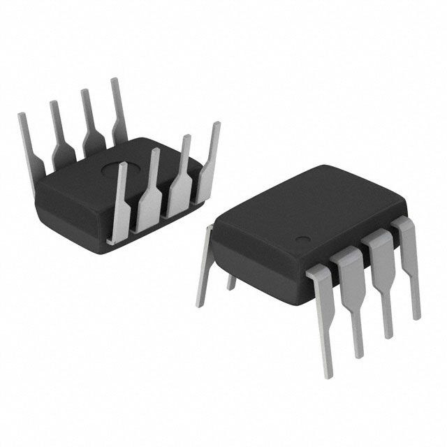
CD40107BE

Why Choose Us?
Professional Platform
B2B & B2C purchasingDelivery at full speed
1-2 days deliveryWide variety
Original manufacturers365 days guarantee
Responsible quality
.png)


Tech Specifications
CD40107BE Description
CD40107BE Description
The CD40107BE is a high-performance NAND gate produced by Texas Instruments. This device is part of the 4000B series and is designed to meet the demands of various electronic applications. With a max propagation delay of 100ns at 15V and 50pF, the CD40107BE offers fast switching capabilities. It operates within a supply voltage range of 3V to 18V, making it suitable for low-power and high-power applications. The device is also REACH unaffected and RoHS3 compliant, ensuring environmental safety and regulatory compliance.
CD40107BE Features
- Logic Type: NAND Gate with 2 inputs and 2 circuits, providing flexible logic operations.
- Max Propagation Delay: 100ns @ 15V, 50pF, ensuring fast signal processing.
- Voltage - Supply: 3V to 18V, supporting a wide range of power supply requirements.
- Input Logic Levels: Low (1.5V to 4V) and High (3.5V to 11V), accommodating various input signal levels.
- Current - Quiescent (Max): 4 µA, minimizing power consumption in standby mode.
- Mounting Type: Through Hole, facilitating easy integration into existing PCB designs.
- Package: Tube, providing a cost-effective and convenient packaging option.
- Features: Open Drain, allowing for easy cascading of multiple gates.
- ECCN: EAR99, indicating export control classification.
- HTSUS: 8542.39.0001, specifying the Harmonized Tariff Schedule code for import/export purposes.
CD40107BE Applications
The CD40107BE is ideal for various applications where fast and reliable logic operations are required. Some specific use cases include:
- Digital Circuits: As a fundamental building block in digital circuits, the CD40107BE can be used to implement complex logic functions.
- Automotive Electronics: The device's wide supply voltage range and low quiescent current make it suitable for automotive applications, such as control units and sensor interfaces.
- Industrial Control Systems: The CD40107BE can be used in industrial control systems to process and manipulate signals from various sensors and actuators.
- Telecommunications: In telecommunications equipment, the CD40107BE can be employed for signal processing and data manipulation tasks.
Conclusion of CD40107BE
The CD40107BE is a versatile and high-performance NAND gate from Texas Instruments. Its unique features, such as fast propagation delay, wide supply voltage range, and open-drain configuration, make it an excellent choice for various electronic applications. With its compliance to environmental regulations and ease of integration, the CD40107BE is a reliable solution for designers looking to implement efficient and robust logic operations in their projects.
FAQ
| Quantity | Unit Price | Ext. Price |
|---|---|---|
| 1+ | $0.60720 | $0.61 |
| 10+ | $0.43384 | $4.34 |
| 50+ | $0.36309 | $18.15 |
| 100+ | $0.34100 | $34.10 |
| 250+ | $0.31768 | $79.42 |
Not available to buy online? Want the lower wholesale price? Please Send RFQ to get best price, we will respond immediately


.png?x-oss-process=image/format,webp/resize,h_32)


