
Texas Instruments
CD4015BPWR
Shift Registers


.png?x-oss-process=image/format,webp/resize,p_30)


CD4015BPWR Description
CD4015BPWR Description
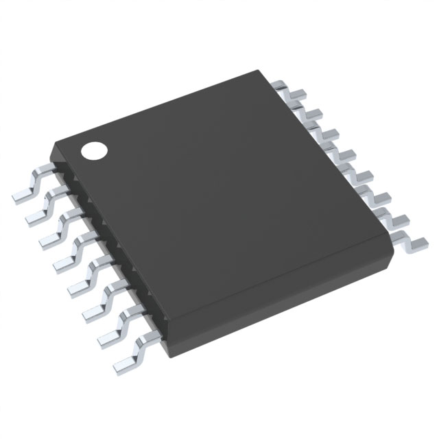
The CD4015BPWR is a high-performance, dual static shift register manufactured by Texas Instruments, designed to meet the demands of modern electronic systems. This device features a 4-bit serial-to-parallel conversion function, allowing for efficient data manipulation and processing in various applications. With a supply voltage range of 3V to 18V, the CD4015BPWR offers flexibility in power requirements, making it suitable for a wide range of electronic devices.
CD4015BPWR Features
- 4-bit per Element: The CD4015BPWR boasts a 4-bit per element configuration, enabling efficient data handling and processing.
- Shift Register Logic Type: As a shift register, the CD4015BPWR is designed to store and manipulate data in a sequential manner, making it ideal for applications requiring data buffering and processing.
- Dual Elements: With two 4-bit shift registers, the CD4015BPWR can handle twice the data volume compared to single-element shift registers, enhancing its versatility and performance.
- Surface Mount Technology: The CD4015BPWR is designed for surface mount applications, allowing for compact and efficient integration into electronic systems.
- Wide Voltage Range: The device operates within a 3V to 18V supply voltage range, providing flexibility in power requirements and compatibility with various electronic systems.
- RoHS Compliance: The CD4015BPWR is compliant with the Restriction of Hazardous Substances (RoHS) directive, ensuring environmental responsibility and adherence to industry standards.
CD4015BPWR Applications
The CD4015BPWR is ideal for a variety of applications where efficient data manipulation and processing are required. Some specific use cases include:
- Data Buffering: In systems requiring temporary data storage and manipulation, the CD4015BPWR can serve as a reliable buffer, ensuring data integrity and facilitating seamless data transfer.
- Serial-to-Parallel Conversion: The CD4015BPWR's 4-bit serial-to-parallel conversion function makes it suitable for applications requiring data format conversion, such as in communication systems and data processing units.
- Digital Signal Processing: In digital signal processing applications, the CD4015BPWR can be used to manipulate and process signals, enabling efficient data handling and analysis.
- Automotive Electronics: The CD4015BPWR's wide voltage range and RoHS compliance make it suitable for automotive electronics, where reliability and environmental responsibility are crucial.
Conclusion of CD4015BPWR
The CD4015BPWR is a versatile and high-performance dual static shift register that offers numerous benefits for modern electronic systems. Its 4-bit per element configuration, shift register logic type, and dual elements provide efficient data manipulation and processing capabilities. With a wide voltage range, surface mount technology, and RoHS compliance, the CD4015BPWR is an ideal choice for a variety of applications, including data buffering, serial-to-parallel conversion, digital signal processing, and automotive electronics.
Tech Specifications
CD4015BPWR Documents
Download datasheets and manufacturer documentation for CD4015BPWR
 CD4015B Types
  CD4015B Types
 Shopping Guide


.png?x-oss-process=image/format,webp/resize,h_32)


