
 German
 Japanese
 Portuguese
 Korea
Korea
 Mexico
 Dutch
Dutch


Texas Instruments
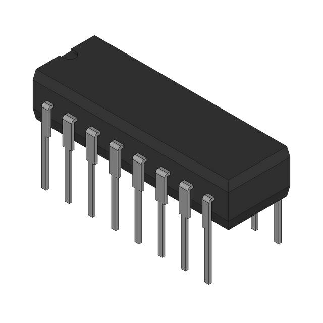
CD40174BF3A

Why Choose Us?
Professional Platform
B2B & B2C purchasingDelivery at full speed
1-2 days deliveryWide variety
Original manufacturers365 days guarantee
Responsible quality
.png)


Tech Specifications
CD40174BF3A Description
CD40174BF3A Description
The CD40174BF3A is a high-performance CMOS HEX D-type flip-flop from Texas Instruments, designed for a wide range of digital applications. This device is part of the CD4000 series, known for its robustness and reliability in various electronic circuits. The CD40174BF3A features six independent D-type flip-flops, each capable of storing a single bit of data. The flip-flops are edge-triggered, ensuring precise timing and synchronization in digital systems.
CD40174BF3A Features
- High-Performance CMOS Technology: The CD40174BF3A leverages advanced CMOS technology, offering low power consumption and high noise immunity. This makes it suitable for both battery-powered and high-noise environments.
- Edge-Triggered Operation: Each flip-flop is edge-triggered, allowing for precise control over data storage and retrieval. This feature is crucial for applications requiring accurate timing and synchronization.
- Independent Flip-Flops: The device comprises six independent D-type flip-flops, providing flexibility in handling multiple data bits simultaneously. This is particularly useful in applications such as data registers and counters.
- Wide Operating Voltage Range: The CD40174BF3A operates over a wide voltage range, typically from 3V to 18V, making it compatible with various power supply configurations.
- Low Power Consumption: The CMOS design ensures minimal power usage, which is essential for extending battery life in portable devices.
- Bulk Packaging: Available in bulk packaging, the CD40174BF3A is ideal for high-volume production and inventory management.
CD40174BF3A Applications
The CD40174BF3A is versatile and finds application in a variety of electronic systems:
- Data Registers: The device's ability to store multiple bits of data makes it ideal for use in data registers, where information needs to be temporarily held for processing.
- Counters: The independent flip-flops can be cascaded to create counters for timing and sequencing applications.
- Memory Buffers: The CD40174BF3A can serve as a memory buffer, temporarily holding data between processing stages in digital systems.
- Control Logic: The flip-flops can be used in control logic circuits to manage the flow of data and control signals in complex systems.
- Communication Systems: In communication systems, the CD40174BF3A can be used for data synchronization and buffering to ensure reliable data transmission.
Conclusion of CD40174BF3A
The CD40174BF3A from Texas Instruments is a reliable and efficient CMOS HEX D-type flip-flop, offering a range of features that make it suitable for various digital applications. Its edge-triggered operation, low power consumption, and wide operating voltage range provide significant advantages over similar models. The device's ability to handle multiple data bits independently makes it a versatile component in digital circuits. Whether used in data registers, counters, or control logic, the CD40174BF3A ensures precise timing and reliable performance. Its bulk packaging and active product status make it an excellent choice for high-volume production and long-term availability.
FAQ
| Quantity | Unit Price | Ext. Price |
|---|---|---|
| 19+ | $13.95680 | $265.18 |
Not available to buy online? Want the lower wholesale price? Please Send RFQ to get best price, we will respond immediately


.png?x-oss-process=image/format,webp/resize,h_32)


