
Texas Instruments
CD4019BF3A
Gates and Inverters


.png?x-oss-process=image/format,webp/resize,p_30)


CD4019BF3A Description
CD4019BF3A Description
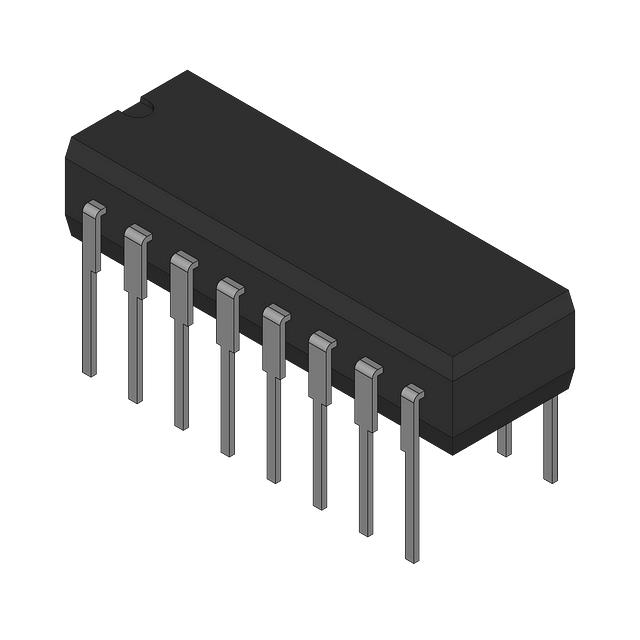
The CD4019BF3A is a CMOS Quad AND/OR Select Gate IC, part of the 4000B series, manufactured by Texas Instruments. This logic IC chip is designed for a wide range of digital applications, offering versatile functionality and robust performance. The device features four independent AND/OR gates, each with two inputs, providing flexibility in digital circuit design. It operates within a supply voltage range of 3V to 18V, making it suitable for various power supply configurations. The CD4019BF3A is housed in a through-hole package, specifically a tube, which ensures reliable mechanical stability and ease of integration into printed circuit boards. The product is currently active and RoHS3 compliant, adhering to stringent environmental standards.
CD4019BF3A Features
- Logic Type: AND/OR Gate, offering dual functionality within a single package.
- Supply Voltage Range: 3V to 18V, providing compatibility with a broad spectrum of power supply voltages.
- Number of Circuits: Four independent AND/OR gates, each with two inputs, enhancing design flexibility.
- Mounting Type: Through-hole, ensuring robust mechanical stability and ease of integration.
- Output Current: 6.8mA for both high and low states, ensuring reliable signal transmission.
- Series: 4000B, a well-established series known for its reliability and performance.
- RoHS Compliance: ROHS3 compliant, meeting environmental standards and ensuring sustainability.
- Package: Tube, providing protection and ease of handling during assembly processes.
CD4019BF3A Applications
The CD4019BF3A is ideal for a variety of digital applications where AND/OR logic functions are required. Its wide supply voltage range and robust design make it suitable for use in:
- Digital Signal Processing: Efficiently processing digital signals in various electronic systems.
- Control Systems: Implementing logic functions in control circuits for automation and robotics.
- Communication Systems: Managing digital signals in communication protocols and interfaces.
- Consumer Electronics: Enhancing functionality in devices such as remote controls, digital displays, and home automation systems.
- Industrial Applications: Utilized in industrial control panels, PLCs, and other digital control systems.
Conclusion of CD4019BF3A
The CD4019BF3A from Texas Instruments is a versatile and reliable CMOS Quad AND/OR Select Gate IC. Its dual functionality, wide supply voltage range, and robust through-hole packaging make it an excellent choice for a variety of digital applications. The device's RoHS3 compliance ensures it meets modern environmental standards, making it a sustainable choice for electronics designers. With its high output current capability and compatibility with a broad range of power supplies, the CD4019BF3A stands out as a reliable and efficient solution for digital circuit design.
Tech Specifications
CD4019BF3A Documents
Download datasheets and manufacturer documentation for CD4019BF3A
Shopping Guide


.png?x-oss-process=image/format,webp/resize,h_32)


