
 German
 Japanese
 Portuguese
 Korea
Korea
 Mexico
 Dutch
Dutch


Texas Instruments
CD4019BNSR

Why Choose Us?
Professional Platform
B2B & B2C purchasingDelivery at full speed
1-2 days deliveryWide variety
Original manufacturers365 days guarantee
Responsible quality
.png)


Tech Specifications
CD4019BNSR Description
CD4019BNSR Description
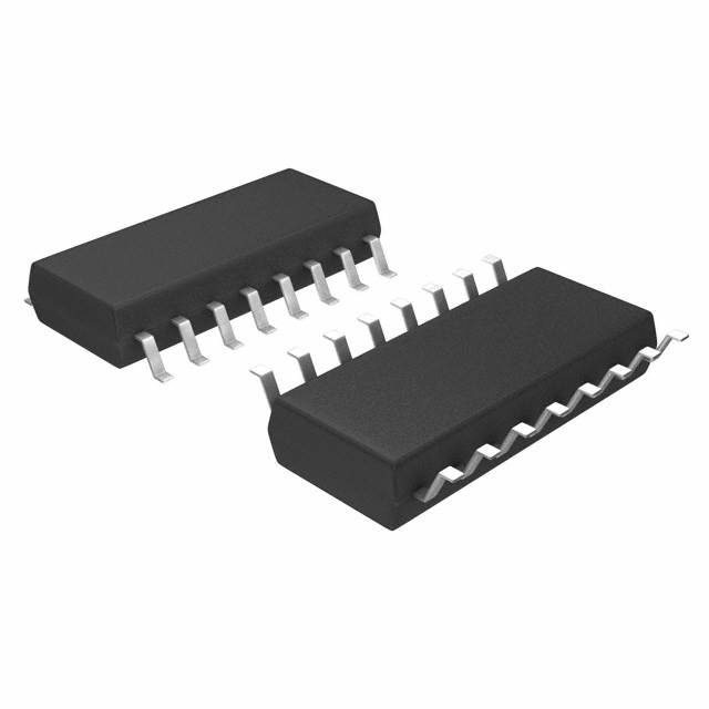
The CD4019BNSR is a Quad AND/OR Select Gate Logic IC Chip, part of the 4000B series, manufactured by Texas Instruments. This versatile IC is designed for surface mount applications, making it suitable for compact and high-density PCB designs. It features four independent circuits, each with two inputs, providing a wide range of logic functions through its AND/OR gate configuration. The CD4019BNSR operates within a supply voltage range of 3V to 18V, ensuring compatibility with various power supply systems. It is packaged in a 16SO (Small Outline) format, further enhancing its suitability for space-constrained applications.
CD4019BNSR Features
- Logic Type: AND/OR Gate
- Mounting Type: Surface Mount
- Series: 4000B
- Voltage - Supply: 3V to 18V
- Number of Inputs: 2 per circuit
- Number of Circuits: 4
- Current - Output High, Low: 6.8mA, 6.8mA
- Moisture Sensitivity Level (MSL): 1 (Unlimited)
- Package: Tape & Reel (TR)
- Product Status: Active
- ECCN: EAR99
- HTSUS: 8542.39.0001
- REACH Status: REACH Unaffected
- RoHS Status: ROHS3 Compliant
The CD4019BNSR offers several unique features that set it apart from similar models. Its wide operating voltage range makes it highly adaptable to different power supply configurations, ensuring reliable performance across various applications. The surface mount package design allows for efficient use of PCB space, making it ideal for modern electronic devices where compactness is crucial. Additionally, the IC's compliance with REACH and RoHS3 standards ensures it meets the highest environmental and safety regulations, making it suitable for global markets.
CD4019BNSR Applications
The CD4019BNSR is well-suited for a variety of applications due to its versatile logic functions and compact design. Some specific use cases include:
- Digital Signal Processing: The AND/OR gate configuration allows for efficient processing of digital signals, making it ideal for applications such as digital filters, signal multiplexing, and data encoding.
- Control Systems: The IC can be used in control systems where multiple inputs need to be processed to generate control, signals such as in motor control, automation, and robotics.
- Communication Systems: In communication systems, the CD4019BNSR can be employed for signal routing, switching, and logic operations, enhancing the efficiency and reliability of data transmission.
- Consumer Electronics: The compact size and surface mount design make it suitable for consumer electronics where space is limited, such as smartphones, tablets, and wearable devices.
Conclusion of CD4019BNSR
The CD4019BNSR is a highly versatile and reliable Quad AND/OR Select Gate Logic IC Chip from Texas Instruments. Its wide operating voltage range, surface mount package, and compliance with environmental standards make it an excellent choice for a variety of applications. Whether used in digital signal processing, control systems, communication systems, or consumer electronics, the CD4019BNSR offers robust performance and adaptability. Its active product status and availability in tape & reel packaging ensure a steady supply for manufacturers, making it a dependable component for modern electronic designs.
FAQ
| Quantity | Unit Price | Ext. Price |
|---|---|---|
| 1+ | $0.51920 | $0.52 |
| 10+ | $0.36608 | $3.66 |
| 25+ | $0.32806 | $8.20 |
| 100+ | $0.28591 | $28.59 |
| 250+ | $0.26583 | $66.46 |
Not available to buy online? Want the lower wholesale price? Please Send RFQ to get best price, we will respond immediately


.png?x-oss-process=image/format,webp/resize,h_32)


