
 German
 Japanese
 Portuguese
 Korea
Korea
 Mexico
 Dutch
Dutch


Texas Instruments
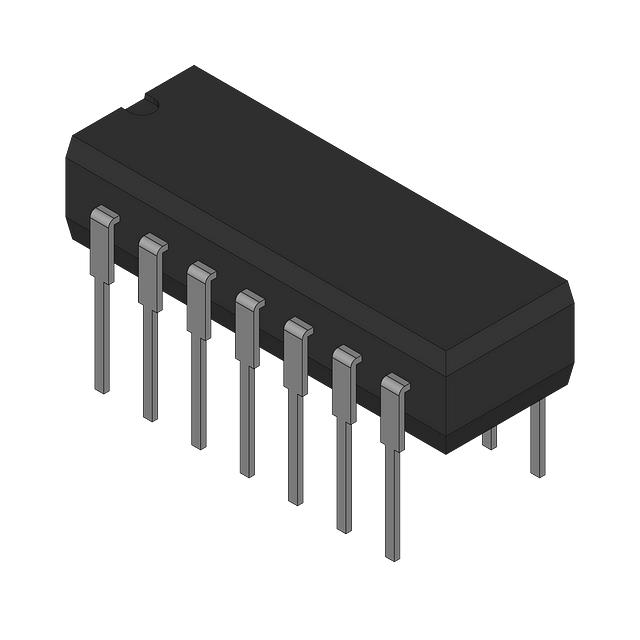
CD4025BF

Why Choose Us?
Professional Platform
B2B & B2C purchasingDelivery at full speed
1-2 days deliveryWide variety
Original manufacturers365 days guarantee
Responsible quality
.png)


Tech Specifications
CD4025BF Description
CD4025BF Description
The CD4025BF is a high-performance, triple 3-input NOR gate logic IC chip manufactured by Texas Instruments. This device is designed to operate within a wide supply voltage range of 3V to 18V, making it highly versatile for various electronic applications. The CD4025BF features a quiescent current of a maximum of 5 µA, ensuring low power consumption even in standby mode. It is available in a through-hole package, which is ideal for applications requiring robust mechanical stability and ease of installation on printed circuit boards.
CD4025BF Features
- Triple 3-Input NOR Gates: The CD4025BF comprises three independent 3-input NOR gates, providing multiple logic functions within a single package.
- Wide Supply Voltage Range: With a supply voltage range of 3V to 18V, the CD4025BF is suitable for a variety of power supply configurations.
- Low Quiescent Current: The maximum quiescent current of 5 µA ensures minimal power consumption, making it ideal for battery-operated and low-power applications.
- High Output Current Capability: The device can deliver up to 6.8mA for both high and low output states, ensuring robust performance in driving various loads.
- Fast Propagation Delay: The maximum propagation delay of 90ns at 15V and 50pF load capacitance ensures high-speed operation, making it suitable for fast digital circuits.
- Input Logic Levels: The CD4025BF supports input logic levels of 1.5V to 4V for low and 3.5V to 11V for high, providing compatibility with a wide range of digital systems.
- Through-Hole Mounting: The through-hole package type ensures reliable mechanical stability and ease of assembly, making it suitable for both prototyping and production environments.
CD4025BF Applications
The CD4025BF is ideal for a wide range of applications due to its versatile features and robust performance. Some specific use cases include:
- Digital Logic Circuits: The triple 3-input NOR gates make the CD4025BF suitable for constructing complex digital logic circuits, such as decoders, multiplexers, and control systems.
- Low-Power Systems: The low quiescent current and wide supply voltage range make it ideal for battery-operated devices and systems requiring minimal power consumption.
- High-Speed Applications: The fast propagation delay ensures that the CD4025BF can be used in high-speed digital systems, such as digital signal processing and communication interfaces.
- Industrial Control Systems: The robust through-hole package and high output current capability make it suitable for industrial control systems and automation applications.
- Consumer Electronics: The CD4025BF can be used in various consumer electronics applications, such as remote controls, home automation systems, and portable devices.
Conclusion of CD4025BF
The CD4025BF from Texas Instruments is a versatile and high-performance logic IC chip that offers multiple benefits over similar models. Its wide supply voltage range, low quiescent current, and high output current capability make it suitable for a variety of applications, from low-power systems to high-speed digital circuits. The fast propagation delay and compatibility with various input logic levels further enhance its performance and versatility. The through-hole package ensures reliable mechanical stability and ease of assembly, making it ideal for both prototyping and production environments. Overall, the CD4025BF is an excellent choice for designers and engineers looking for a reliable and high-performance NOR gate logic IC.
FAQ
Not available to buy online? Want the lower wholesale price? Please Send RFQ to get best price, we will respond immediately


.png?x-oss-process=image/format,webp/resize,h_32)


