
 German
 Japanese
 Portuguese
 Korea
Korea
 Mexico
 Dutch
Dutch


Texas Instruments
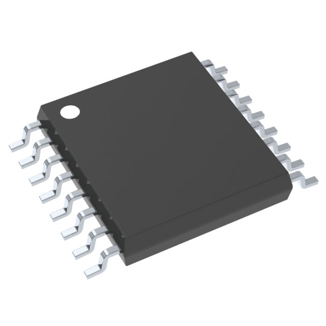
CD4042BPW

Why Choose Us?
Professional Platform
B2B & B2C purchasingDelivery at full speed
1-2 days deliveryWide variety
Original manufacturers365 days guarantee
Responsible quality
.png)


Tech Specifications
CD4042BPW Description
CD4042BPW Description
The CD4042BPW is a high-performance, quad clocked D latch designed for a wide range of electronic applications. Manufactured by Texas Instruments, this IC belongs to the 4000B series and is housed in a 16TSSOP package. It features differential outputs, providing robust performance in various electronic circuits. The CD4042BPW operates within a supply voltage range of 3V to 18V, making it versatile for different power supply configurations. With a propagation delay time of 40ns, it ensures rapid signal processing and synchronization. The device is REACH unaffected and RoHS3 compliant, adhering to stringent environmental and safety standards. It also has a moisture sensitivity level (MSL) of 1, indicating unlimited storage conditions, which enhances its reliability and longevity.
CD4042BPW Features
- Differential Outputs: The CD4042BPW offers differential outputs, which provide enhanced signal integrity and noise immunity, making it ideal for high-speed and high-reliability applications.
- Quad Clocked D Latch: This device features four independent 1:1 clocked D latches, allowing for efficient data storage and transfer in digital circuits.
- Wide Supply Voltage Range: The CD4042BPW operates within a supply voltage range of 3V to 18V, providing flexibility in power supply requirements and compatibility with various electronic systems.
- Low Propagation Delay: With a propagation delay of 40ns, the CD4042BPW ensures fast signal processing and synchronization, making it suitable for high-speed digital applications.
- High Output Current: The device can source and sink up to 6.8mA, providing robust performance and compatibility with a wide range of load conditions.
- Surface Mount Technology: The CD4042BPW is designed for surface mount applications, enabling compact and efficient PCB layouts.
- Environmental Compliance: The CD4042BPW is REACH unaffected and RoHS3 compliant, ensuring it meets stringent environmental and safety standards.
- Unlimited Moisture Sensitivity Level: With an MSL of 1, the CD4042BPW can be stored under unlimited conditions, enhancing its reliability and longevity.
CD4042BPW Applications
The CD4042BPW is ideal for a variety of applications due to its robust performance and versatile features. Some specific use cases include:
- Digital Logic Circuits: The quad clocked D latches make the CD4042BPW suitable for digital logic circuits, where data storage and transfer are critical.
- High-Speed Data Processing: The low propagation delay of 40ns ensures rapid signal processing, making it ideal for high-speed data processing applications.
- Noise-Sensitive Environments: The differential outputs provide enhanced signal integrity and noise immunity, making the CD4042BPW suitable for applications in noisy environments.
- Power-Efficient Systems: The wide supply voltage range allows for compatibility with various power supply configurations, making it ideal for power-efficient systems.
- Surface Mount Applications: The surface mount technology enables compact and efficient PCB layouts, making the CD4042BPW suitable for applications where space is a constraint.
Conclusion of CD4042BPW
The CD4042BPW from Texas Instruments is a versatile and high-performance quad clocked D latch, offering differential outputs, a wide supply voltage range, and low propagation delay. Its robust features, including high output current, surface mount technology, and environmental compliance, make it suitable for a wide range of applications. Whether used in digital logic circuits, high-speed data processing, or noise-sensitive environments, the CD4042BPW provides reliable performance and enhanced signal integrity. Its compatibility with various power supply configurations and compact design make it an ideal choice for modern electronic systems.
FAQ
| Quantity | Unit Price | Ext. Price |
|---|---|---|
| 1+ | $0.96800 | $0.97 |
| 10+ | $0.69872 | $6.99 |
| 90+ | $0.56183 | $50.56 |
| 180+ | $0.53347 | $96.02 |
| 270+ | $0.51926 | $140.20 |
Not available to buy online? Want the lower wholesale price? Please Send RFQ to get best price, we will respond immediately


.png?x-oss-process=image/format,webp/resize,h_32)


