
 German
 Japanese
 Portuguese
 Korea
Korea
 Mexico
 Dutch
Dutch


Texas Instruments
CD4043BDWR

Why Choose Us?
Professional Platform
B2B & B2C purchasingDelivery at full speed
1-2 days deliveryWide variety
Original manufacturers365 days guarantee
Responsible quality
.png)


Tech Specifications
CD4043BDWR Description
CD4043BDWR Description
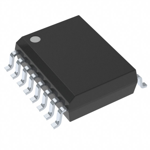
The CD4043BDWR from Texas Instruments is a high-performance Quad NOR R/S Latch with 3-State Outputs, designed for robust digital logic applications. Part of the 4000B series, it operates across a wide voltage range of 3V to 18V, making it versatile for both low-power and industrial-level designs. Housed in a 16-SOIC package with surface-mount compatibility, this latch is ideal for compact PCB layouts. Its 50ns propagation delay ensures efficient signal processing, while the 6.8mA output current (both high and low) supports moderate drive requirements. Compliant with ROHS3 and REACH standards, it is suitable for environmentally conscious designs.
CD4043BDWR Features
- Quad NOR R/S Latches: Four independent 1:1 latches with NOR-based set/reset functionality.
- 3-State Outputs: Allows bus-oriented applications by enabling high-impedance states.
- Wide Voltage Range (3V–18V): Compatible with TTL and CMOS logic levels.
- Balanced Output Drive (6.8mA): Ensures reliable signal integrity in mixed-load conditions.
- Low Propagation Delay (50ns): Enhances timing performance in sequential logic circuits.
- Surface-Mount 16-SOIC Package: Optimized for space-constrained designs.
- Robust Compliance: ROHS3, REACH Unaffected, and MSL 1 (Unlimited) for reliability in harsh environments.
CD4043BDWR Applications
The CD4043BDWR excels in systems requiring state retention, signal gating, or bus interfacing, such as:
- Data Storage Systems: Used in register banks or temporary memory buffers.
- Industrial Control Logic: Ideal for PLCs and machinery sequencing.
- Communication Interfaces: Facilitates bus arbitration in multi-master systems.
- Power Management: Enables clean signal latching in voltage monitoring circuits.
- Automotive Electronics: Suitable for non-critical control modules due to its wide voltage tolerance.
Conclusion of CD4043BDWR
The CD4043BDWR stands out for its versatility, reliability, and ease of integration in digital systems. Its 3-state outputs and NOR-based latch design provide flexibility for complex logic architectures, while the wide supply range ensures compatibility across diverse applications. Whether for industrial automation, data handling, or embedded control, this latch delivers consistent performance with Texas Instruments' quality assurance. A dependable choice for engineers prioritizing efficiency and compliance in modern electronics.
FAQ
| Quantity | Unit Price | Ext. Price |
|---|---|---|
| 1+ | $0.66000 | $0.66 |
| 10+ | $0.47168 | $4.72 |
| 25+ | $0.42381 | $10.60 |
| 100+ | $0.37118 | $37.12 |
| 250+ | $0.34616 | $86.54 |
Not available to buy online? Want the lower wholesale price? Please Send RFQ to get best price, we will respond immediately


.png?x-oss-process=image/format,webp/resize,h_32)


