
 German
 Japanese
 Portuguese
 Korea
Korea
 Mexico
 Dutch
Dutch


Texas Instruments
CD4049UBDWR
705-CD4049UBDWR

PDF Datasheet
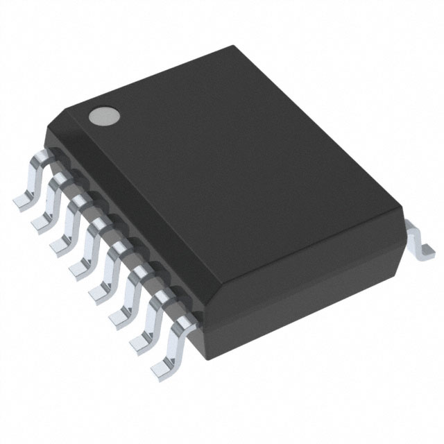
CMOS Hex Inverter Buffer SOIC 6-Bit 20V Surface Mount
Why Choose Us?
Professional Platform
B2B & B2C purchasingDelivery at full speed
1-2 days deliveryWide variety
Original manufacturers365 days guarantee
Responsible quality
.png)


Tech Specifications
Package/Case
SOIC
Contact Plating
Gold
High Level Output Current
-5.2mA
Lead Free
Contains Lead
Logic Function
Buffer, Inverter
Low Level Output Current
25mA
Max Operating Temperature
125°C
Min Operating Temperature
-55°C
CD4049UBDWR Description
Inverter IC 6 Channel 16-SOIC
FAQ
Is CD4049UBDWR currently in stock?
CD4049UBDWR is currently available on an inquiry basis. Please contact us for the latest stock information.
Does CD4049UBDWR have quantity-based pricing?
What operating temperature range does CD4049UBDWR support?
What package or case is CD4049UBDWR available in?
What voltage specification is listed for CD4049UBDWR?
Quick Quote
ADD TO RFQ LIST
Not available to buy online? Want the lower wholesale price? Please Send RFQ to get best price, we will respond immediately
QUICK RFQ


.png?x-oss-process=image/format,webp/resize,h_32)


