
 German
 Japanese
 Portuguese
 Korea
Korea
 Mexico
 Dutch
Dutch


Texas Instruments
CD4050BDWR

Why Choose Us?
Professional Platform
B2B & B2C purchasingDelivery at full speed
1-2 days deliveryWide variety
Original manufacturers365 days guarantee
Responsible quality
.png)


Tech Specifications
CD4050BDWR Description
CD4050BDWR Description
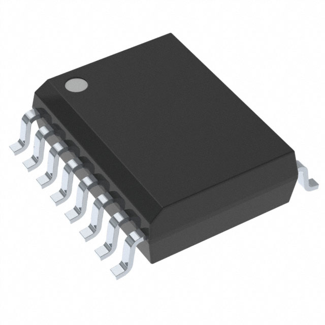
The CD4050BDWR is a non-inverting buffer IC designed by Texas Instruments, part of the 4000B series. This device is engineered to provide robust performance with a wide supply voltage range of 3V to 18V. It features six independent buffer elements, each capable of handling one bit of data. The CD4050BDWR is packaged in a 16-lead small outline integrated circuit (SOIC) and is available in a tape and reel format, making it suitable for surface mount applications. This IC is compliant with the latest RoHS3 standards and is REACH unaffected, ensuring it meets stringent environmental and safety regulations.
CD4050BDWR Features
- Wide Supply Voltage Range: The CD4050BDWR operates within a supply voltage range of 3V to 18V, making it versatile for various power supply configurations.
- High Output Current Capability: Each buffer element can source up to 8mA and sink up to 48mA, providing robust performance for driving various loads.
- Non-Inverting Buffers: The six buffer elements are non-inverting, ensuring that the output signal maintains the same logical state as the input signal.
- Surface Mount Compatibility: The 16SOIC package is ideal for surface mount technology (SMT), facilitating efficient and reliable assembly processes.
- Environmental Compliance: The CD4050BDWR is RoHS3 compliant and REACH unaffected, ensuring it meets the latest environmental and safety standards.
- Low Moisture Sensitivity: With a moisture sensitivity level (MSL) of 1, the CD4050BDWR is suitable for unlimited storage and handling conditions, reducing the risk of moisture-related damage.
CD4050BDWR Applications
The CD4050BDWR is ideal for a variety of applications where signal buffering and voltage level translation are required. Some specific use cases include:
- Digital Signal Processing: The non-inverting buffers can be used to amplify and condition digital signals in microcontroller and microprocessor systems.
- Voltage Level Translation: The wide supply voltage range allows the CD4050BDWR to translate signals between different voltage levels, facilitating communication between devices with varying power requirements.
- Logic Circuitry: The IC can be employed in complex logic circuits to ensure signal integrity and reduce noise.
- Consumer Electronics: The CD4050BDWR is suitable for applications in consumer electronics where compact size and high reliability are crucial.
- Industrial Control Systems: The robustness and wide operating voltage range make it ideal for industrial applications where reliability and durability are paramount.
Conclusion of CD4050BDWR
The CD4050BDWR from Texas Instruments is a versatile and reliable non-inverting buffer IC that offers a wide range of features and benefits. Its wide supply voltage range, high output current capability, and compliance with environmental regulations make it an excellent choice for a variety of applications. Whether used in digital signal processing, voltage level translation, or complex logic circuits, the CD4050BDWR provides dependable performance and ensures signal integrity. Its surface mount compatibility and low moisture sensitivity further enhance its suitability for modern electronics manufacturing processes.
FAQ
| Quantity | Unit Price | Ext. Price |
|---|---|---|
| 1+ | $0.63772 | $0.64 |
| 10+ | $0.51943 | $5.19 |
| 30+ | $0.46115 | $13.83 |
| 100+ | $0.40285 | $40.28 |
Not available to buy online? Want the lower wholesale price? Please Send RFQ to get best price, we will respond immediately


.png?x-oss-process=image/format,webp/resize,h_32)


