
 German
 Japanese
 Portuguese
 Korea
Korea
 Mexico
 Dutch
Dutch


Texas Instruments
CD4053BPWRG3
747-CD4053BPWRG3

PDF Datasheet
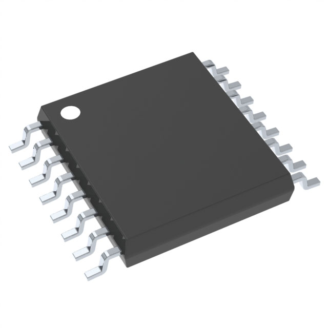
3-Ch Analog Mux/Demux, 20V, 30MHz, 16-TSSOP, SMT
20 Weeks
Why Choose Us?
Professional Platform
B2B & B2C purchasingDelivery at full speed
1-2 days deliveryWide variety
Original manufacturers365 days guarantee
Responsible quality
.png)


Tech Specifications
-3db Bandwidth
30MHz
Bandwidth
30MHz
Package/Case
TSSOP
Contact Plating
Tin
Lead Free
Lead Free
Logic Function
Multiplexer, Demultiplexer
Max Dual Supply Voltage
9V
Min Dual Supply Voltage
2.5V
CD4053BPWRG3 Description
3 Circuit IC Switch 2:1 240Ohm 16-TSSOP
FAQ
What is the mounting type of CD4053BPWRG3?
CD4053BPWRG3 uses a Surface Mount mounting style based on the listed product specifications.
What voltage specification is listed for CD4053BPWRG3?
What is CD4053BPWRG3?
What operating temperature range does CD4053BPWRG3 support?
What is the standard lead time for CD4053BPWRG3?
Availability
(In Stock :
7722 )
| Quantity | Unit Price | Ext. Price |
|---|---|---|
| 1+ | $0.66880 | $0.67 |
| 10+ | $0.47520 | $4.75 |
| 25+ | $0.42698 | $10.67 |
| 100+ | $0.37409 | $37.41 |
| 250+ | $0.34887 | $87.22 |
Quick Quote
ADD TO RFQ LIST
Not available to buy online? Want the lower wholesale price? Please Send RFQ to get best price, we will respond immediately
QUICK RFQ


.png?x-oss-process=image/format,webp/resize,h_32)


