
 German
 Japanese
 Portuguese
 Korea
Korea
 Mexico
 Dutch
Dutch


Texas Instruments
CD4067BM

Why Choose Us?
Professional Platform
B2B & B2C purchasingDelivery at full speed
1-2 days deliveryWide variety
Original manufacturers365 days guarantee
Responsible quality
.png)


Tech Specifications
CD4067BM Description
CD4067BM Description
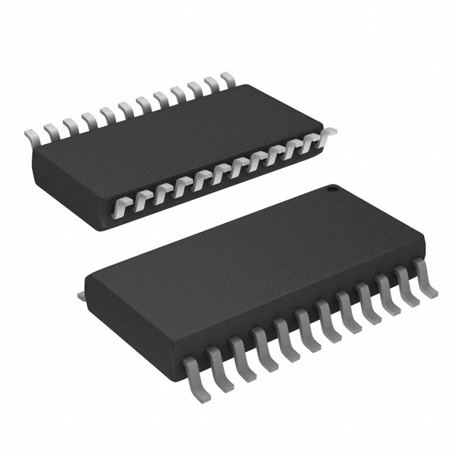
The CD4067BM from Texas Instruments is a high-performance 16:1 analog multiplexer/demultiplexer IC designed for precision signal routing in low-to-medium frequency applications. Housed in a 24-SOIC package, it features a wide supply voltage range (3V to 18V) and low on-state resistance (240Ω max), making it suitable for both industrial and consumer electronics. With a -3dB bandwidth of 14MHz and minimal channel-to-channel matching (ΔRon: 5Ω), it ensures consistent signal integrity across all channels. The device is RoHS3 compliant and has a low leakage current (100nA max), enhancing reliability in battery-powered systems.
CD4067BM Features
- Low On-Resistance: 240Ω max ensures minimal signal attenuation.
- High Bandwidth: 14MHz -3dB supports moderate-speed analog signals.
- Low Leakage: 100nA max (IS(off)) reduces power loss in standby modes.
- Low Capacitance: 0.2pF (CS(off)), 55pF (CD(off)) minimizes crosstalk.
- Wide Voltage Range: 3V to 18V compatibility for versatile designs.
- 16:1 Channel Configuration: Ideal for complex signal routing.
- Robust Packaging: 24-SOIC with MSL 1 (Unlimited) moisture sensitivity.
CD4067BM Applications
- Data Acquisition Systems: Multiplexing sensor inputs with low distortion.
- Audio/Video Switching: High-fidelity signal routing in AV equipment.
- Battery-Powered Devices: Low leakage extends battery life.
- Test & Measurement: Precision channel selection in automated test setups.
- Industrial Control: Reliable signal switching in harsh environments.
Conclusion of CD4067BM
The CD4067BM stands out for its low on-resistance, wide voltage range, and excellent channel matching, making it a top choice for analog signal routing. Its low power consumption and high bandwidth cater to demanding applications in industrial, automotive, and consumer electronics. While classified as Last Time Buy, its performance and reliability ensure it remains a preferred solution for legacy and new designs requiring robust multiplexing capabilities.
FAQ
| Quantity | Unit Price | Ext. Price |
|---|---|---|
| 1+ | $0.67543 | $0.68 |
| 10+ | $0.54172 | $5.42 |
| 25+ | $0.47485 | $11.87 |
Not available to buy online? Want the lower wholesale price? Please Send RFQ to get best price, we will respond immediately


.png?x-oss-process=image/format,webp/resize,h_32)


