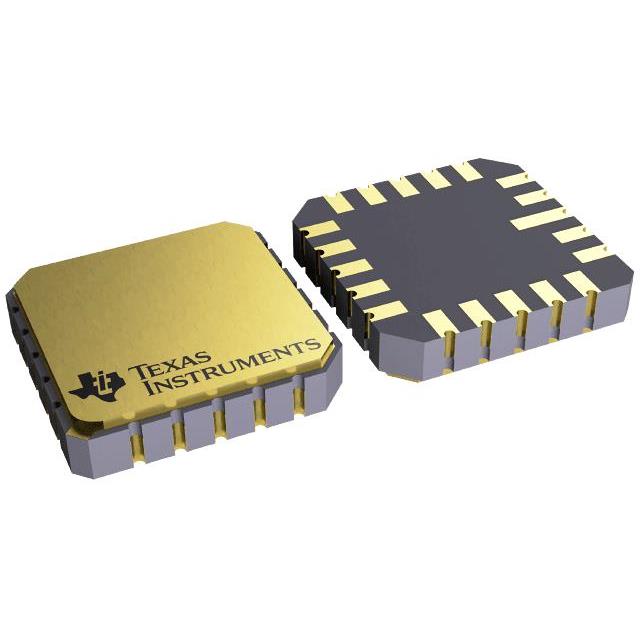

Texas Instruments
CD4085BF3A
Multi-Function, Configurable Gates and Inverters


.png?x-oss-process=image/format,webp/resize,p_30)


CD4085BF3A Description
CD4085BF3A Description
The CD4085BF3A is a CMOS dual 2-wide 2-input AND-OR-Invert gate, designed for versatile logic operations in a wide range of electronic applications. Manufactured by Texas Instruments, this device is part of the Multi-Function, Configurable Gates and Inverters category. It features a robust through-hole mounting type, making it suitable for both prototyping and production environments. The CD4085BF3A is housed in a tube package, ensuring ease of handling and storage.
This gate is designed to operate within a wide supply voltage range of 3V to 18V, providing flexibility in power supply options. It consists of two identical circuits, each with four 2-input gates, allowing for complex logic functions to be implemented in a compact form factor. The device is compliant with ROHS3 standards, ensuring environmental sustainability and regulatory adherence.
CD4085BF3A Features
- Logic Type: The CD4085BF3A integrates AND, OR, and INVERT logic functions, offering a high degree of configurability and versatility in logic design.
- Supply Voltage Range: With a wide operating voltage range of 3V to 18V, this device is suitable for various power supply configurations, enhancing its application scope.
- Through-Hole Mounting: The through-hole mounting type ensures robust mechanical stability and is ideal for applications requiring high reliability and ease of installation.
- High Output Current: The device can provide up to 6.8mA for both high and low outputs, ensuring strong signal drive capabilities.
- Multiple Inputs: The CD4085BF3A features eight inputs (2, 2, 2, 2) across its two circuits, allowing for complex logic functions to be implemented efficiently.
- ROHS3 Compliance: The device adheres to ROHS3 standards, ensuring compliance with environmental regulations and promoting sustainable manufacturing practices.
- Non-Schmitt Trigger Input: The absence of Schmitt trigger inputs ensures precise and stable logic levels, suitable for applications requiring high accuracy.
CD4085BF3A Applications
The CD4085BF3A is ideal for a variety of applications due to its versatile logic functions and robust design. Some specific use cases include:
- Digital Logic Circuits: The AND-OR-Invert gates are perfect for implementing complex digital logic functions in microcontroller peripherals, digital signal processing, and other digital systems.
- Control Systems: The device's high output current and wide voltage range make it suitable for driving control signals in industrial automation, robotics, and other control applications.
- Signal Processing: The CD4085BF3A can be used in signal processing applications where precise logic operations are required, such as in communication systems and data acquisition devices.
- Consumer Electronics: The compact form factor and through-hole mounting type make it suitable for consumer electronics where space is limited, but reliability is crucial.
Conclusion of CD4085BF3A
The CD4085BF3A from Texas Instruments is a versatile and reliable CMOS dual 2-wide 2-input AND-OR-Invert gate, offering a wide range of technical specifications and performance benefits. Its wide supply voltage range, high output current, and multiple input configurations make it suitable for a variety of applications in the electronics industry. The device's compliance with ROHS3 standards ensures environmental sustainability, while its through-hole mounting type provides robust mechanical stability. The CD4085BF3A is an excellent choice for engineers and designers looking for a reliable and versatile logic gate solution.
Tech Specifications
CD4085BF3A Documents
Download datasheets and manufacturer documentation for CD4085BF3A
 CD4085B
 Shopping Guide


.png?x-oss-process=image/format,webp/resize,h_32)


