
Texas Instruments
CD4086BF3A
Multi-Function, Configurable Gates and Inverters


.png?x-oss-process=image/format,webp/resize,p_30)


CD4086BF3A Description
CD4086BF3A Description
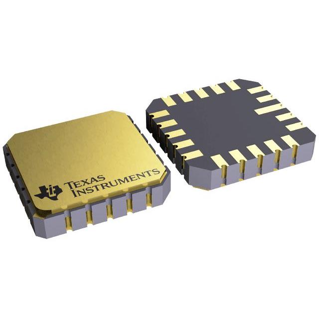
The CD4086BF3A is a CMOS expandable 4-wide 2-input AND/OR/INVERT gate logic IC chip, part of the 4000B series, manufactured by Texas Instruments. This versatile logic IC is designed for a wide range of digital applications, offering robust performance and compatibility with various electronic systems. The CD4086BF3A features an AND/OR/INVERT gate logic type, making it suitable for complex digital signal processing tasks. It operates within a supply voltage range of 3V to 18V, providing flexibility in power requirements. The device is packaged in a through-hole format, making it ideal for applications requiring a reliable and secure mounting method. With a total of 8 inputs (2, 2, 2, 2) and a single circuit configuration, the CD4086BF3A is designed to handle multiple input signals efficiently. It offers a current output of 6.8mA for both high and low states, ensuring stable signal transmission. The CD4086BF3A is also RoHS3 compliant, adhering to stringent environmental standards and ensuring compatibility with modern manufacturing processes.
CD4086BF3A Features
The CD4086BF3A from Texas Instruments offers several unique features that set it apart from similar models in the market:
- AND/OR/INVERT Gate Logic: This versatile logic type allows for a wide range of digital signal processing tasks, making it suitable for various applications.
- Wide Voltage Range: Operating within a supply voltage range of 3V to 18V, the CD4086BF3A provides flexibility in power requirements, ensuring compatibility with different power sources.
- Through-Hole Mounting: The through-hole package ensures a secure and reliable mounting method, making it ideal for applications requiring robust physical stability.
- Multiple Inputs: With a total of 8 inputs (2, 2, 2, 2), the CD4086BF3A can handle multiple input signals efficiently, enhancing its versatility in digital circuits.
- High Current Output: The device offers a current output of 6.8mA for both high and low states, ensuring stable signal transmission and compatibility with various load conditions.
- RoHS3 Compliance: The CD4086BF3A is RoHS3 compliant, adhering to stringent environmental standards and ensuring compatibility with modern manufacturing processes.
CD4086BF3A Applications
The CD4086BF3A is ideal for a variety of applications due to its versatile logic type and robust performance. Some specific use cases include:
- Digital Signal Processing: The AND/OR/INVERT gate logic makes it suitable for complex digital signal processing tasks, such as data encoding and decoding.
- Control Systems: The wide voltage range and high current output make it ideal for use in control systems, where reliable and stable signal transmission is crucial.
- Consumer Electronics: The through-hole mounting and RoHS3 compliance ensure compatibility with modern consumer electronics manufacturing processes.
- Industrial Applications: The robust physical stability provided by the through-hole package makes it suitable for industrial applications where durability is essential.
Conclusion of CD4086BF3A
In conclusion, the CD4086BF3A from Texas Instruments is a versatile and robust logic IC chip, offering a wide range of technical specifications and performance benefits. Its AND/OR/INVERT gate logic, wide voltage range, and multiple input capabilities make it suitable for various digital applications. The through-hole mounting and RoHS3 compliance ensure compatibility with modern manufacturing processes and environmental standards. Whether used in digital signal processing, control systems, consumer electronics, or industrial applications, the CD4086BF3A provides reliable and efficient performance, making it an ideal choice for engineers and designers in the electronics industry.
Tech Specifications
CD4086BF3A Documents
Download datasheets and manufacturer documentation for CD4086BF3A
 CD4086B
 Shopping Guide


.png?x-oss-process=image/format,webp/resize,h_32)


