
 German
 Japanese
 Portuguese
 Korea
Korea
 Mexico
 Dutch
Dutch


Texas Instruments
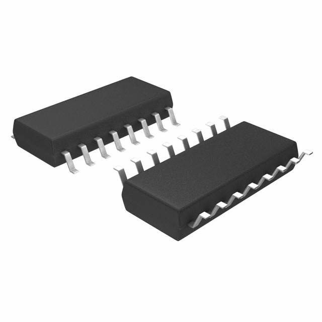
CD4099BNSR

Why Choose Us?
Professional Platform
B2B & B2C purchasingDelivery at full speed
1-2 days deliveryWide variety
Original manufacturers365 days guarantee
Responsible quality
.png)


Tech Specifications
CD4099BNSR Description
CD4099BNSR Description
The CD4099BNSR is a high-performance, 8-bit addressable latch designed for a wide range of digital applications. Manufactured by Texas Instruments, this logic IC chip is part of the 4000B series and features a 1:8 circuit configuration with a single independent circuit. It is designed for surface-mount applications, ensuring compatibility with modern printed circuit board (PCB) designs. The CD4099BNSR operates within a supply voltage range of 3V to 18V, providing flexibility for various power supply requirements.
CD4099BNSR Features
- Standard Output Type: The CD4099BNSR offers a standard output type, ensuring compatibility with a wide range of digital systems.
- Wide Supply Voltage Range: With a supply voltage range of 3V to 18V, this IC can be used in diverse applications without requiring specific voltage levels.
- Low Propagation Delay: The 50ns delay time ensures fast signal propagation, making it suitable for high-speed digital circuits.
- High Output Current Capability: The CD4099BNSR can deliver up to 6.8mA for both high and low outputs, providing robust performance in driving various loads.
- Surface-Mount Packaging: The surface-mount technology (SMT) package allows for efficient PCB design and manufacturing processes.
- Compliance and Standards: The CD4099BNSR is REACH unaffected and RoHS3 compliant, ensuring it meets environmental and safety standards.
- Moisture Sensitivity Level: With an MSL of 1 (unlimited), the CD4099BNSR is highly resistant to moisture, making it suitable for a variety of environmental conditions.
- Packaging: Available in tape and reel (TR) packaging, the CD4099BNSR is ideal for automated assembly processes.
CD4099BNSR Applications
The CD4099BNSR is ideal for applications requiring high-speed, reliable digital signal processing. Its 8-bit addressable latch functionality makes it suitable for:
- Memory Address Decoding: The CD4099BNSR can be used to decode memory addresses in microprocessor systems, ensuring efficient data access.
- Data Latching: It can temporarily store data in digital systems, providing a stable interface between different components.
- Control Logic: The IC can be used in control logic circuits, managing the flow of data and signals in complex systems.
- Communication Interfaces: The CD4099BNSR can be employed in communication interfaces, facilitating data transmission and reception.
- Consumer Electronics: Its wide voltage range and high output current capability make it suitable for various consumer electronics applications, such as televisions, gaming consoles, and home automation systems.
Conclusion of CD4099BNSR
The CD4099BNSR from Texas Instruments is a versatile and reliable 8-bit addressable latch IC, offering a wide supply voltage range, low propagation delay, and high output current capability. Its surface-mount packaging and compliance with environmental standards make it an ideal choice for modern digital systems. Whether used in memory address decoding, data latching, or control logic, the CD4099BNSR provides a robust and efficient solution for a variety of applications.
FAQ
| Quantity | Unit Price | Ext. Price |
|---|---|---|
| 1+ | $0.73920 | $0.74 |
| 10+ | $0.52976 | $5.30 |
| 25+ | $0.47661 | $11.92 |
| 100+ | $0.41844 | $41.84 |
| 250+ | $0.39072 | $97.68 |
Not available to buy online? Want the lower wholesale price? Please Send RFQ to get best price, we will respond immediately


.png?x-oss-process=image/format,webp/resize,h_32)


