
 German
 Japanese
 Portuguese
 Korea
Korea
 Mexico
 Dutch
Dutch


Texas Instruments
CD54AC112F3A

Why Choose Us?
Professional Platform
B2B & B2C purchasingDelivery at full speed
1-2 days deliveryWide variety
Original manufacturers365 days guarantee
Responsible quality
.png)


Tech Specifications
CD54AC112F3A Description
CD54AC112F3A Description
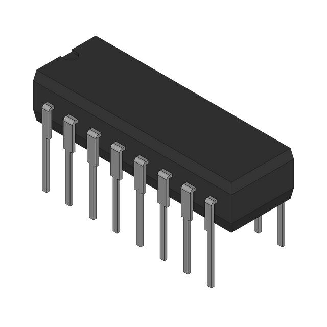
The CD54AC112F3A is a dual negative edge-triggered J-K flip-flop designed by Texas Instruments, a leading manufacturer in the semiconductor industry. This flip-flop is part of the 54AC series and offers a robust and reliable solution for digital circuit applications. It features a clock frequency of 100 MHz, ensuring high-speed operation suitable for demanding applications. The maximum propagation delay is 10.3 ns at 5V and a maximum load capacitance of 50 pF, which guarantees precise timing control. The device operates within a supply voltage range of 1.5V to 5.5V, providing flexibility in power supply requirements.
CD54AC112F3A Features
- High-Speed Performance: With a clock frequency of 100 MHz, the CD54AC112F3A is capable of handling high-speed digital signals, making it ideal for applications requiring rapid data processing and synchronization.
- Low Power Consumption: The quiescent current (Iq) is only 4 µA, which is significantly lower compared to similar models. This feature makes the CD54AC112F3A highly energy-efficient, reducing power consumption and heat generation.
- Complementary Outputs: The device provides complementary outputs, which can be useful for driving differential circuits or reducing the need for additional inverting logic.
- Negative Edge Triggering: The negative edge-triggered design ensures reliable operation in applications where precise timing and synchronization are critical.
- Wide Operating Voltage Range: The supply voltage range of 1.5V to 5.5V allows for compatibility with various power supply systems, enhancing the versatility of the CD54AC112F3A in different electronic designs.
- Set and Reset Functionality: The flip-flop includes set (preset) and reset functions, enabling additional control over the state of the flip-flop, which can be crucial in complex digital systems.
- Through Hole Mounting: The through-hole mounting type ensures robust mechanical stability and ease of integration into printed circuit boards (PCBs).
- ROHS3 Compliant: The CD54AC112F3A is ROHS3 compliant, meeting environmental standards and ensuring that the device is suitable for use in environmentally conscious designs.
- High Current Capability: The output current capability of 24mA for both high and low states ensures robust driving capabilities for various loads.
CD54AC112F3A Applications
The CD54AC112F3A is well-suited for a variety of applications in the electronics industry, including:
- Digital Logic Circuits: Ideal for use in digital systems where precise timing and control are required, such as in counters, dividers, and state machines.
- Data Processing: High-speed operation makes it suitable for data processing applications, ensuring efficient handling of digital signals.
- Synchronization Circuits: The negative edge-triggered design is beneficial for synchronization circuits, where precise timing is critical.
- Memory and Storage Devices: The set and reset functions can be utilized in memory and storage devices to manage data states effectively.
- Communication Systems: The device's high-speed capabilities make it suitable for communication systems where rapid data transmission and processing are necessary.
Conclusion of CD54AC112F3A
The CD54AC112F3A from Texas Instruments is a high-performance dual negative edge-triggered J-K flip-flop that offers a combination of speed, low power consumption, and versatility. Its wide operating voltage range, complementary outputs, and negative edge-triggering make it a reliable choice for a variety of digital applications. The low quiescent current and high current capability further enhance its performance, making it an ideal component for modern digital systems. Whether used in data processing, synchronization circuits, or communication systems, the CD54AC112F3A provides a robust and efficient solution, ensuring reliable operation and precise control.
FAQ
| Quantity | Unit Price | Ext. Price |
|---|---|---|
| 10+ | $26.25040 | $262.50 |
Not available to buy online? Want the lower wholesale price? Please Send RFQ to get best price, we will respond immediately


.png?x-oss-process=image/format,webp/resize,h_32)


