
 German
 Japanese
 Portuguese
 Korea
Korea
 Mexico
 Dutch
Dutch


Texas Instruments
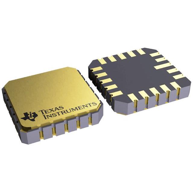
CD54HC74F3A

Why Choose Us?
Professional Platform
B2B & B2C purchasingDelivery at full speed
1-2 days deliveryWide variety
Original manufacturers365 days guarantee
Responsible quality
.png)


Tech Specifications
CD54HC74F3A Description
CD54HC74F3A Description
The CD54HC74F3A is a high-speed CMOS logic dual positive-edge triggered D-type flip-flop with set (preset) and reset functions, designed by Texas Instruments. This logic IC chip is part of the 54HC series, known for its robust performance and reliability. The CD54HC74F3A operates within a supply voltage range of 2V to 6V, making it suitable for a variety of power supply configurations. It features a clock frequency of up to 35 MHz, ensuring fast operation and high-speed data handling capabilities.
CD54HC74F3A Features
- High-Speed Operation: With a maximum clock frequency of 35 MHz, the CD54HC74F3A ensures rapid data processing and minimal latency, making it ideal for high-speed digital systems.
- Low Propagation Delay: The maximum propagation delay is 34ns at 6V and 50pF, which is significantly lower than many comparable models, enhancing the overall system performance.
- Low Quiescent Current: The device consumes only 4 µA in quiescent mode, which is crucial for applications where power efficiency is paramount.
- Complementary Outputs: The CD54HC74F3A provides complementary outputs, offering flexibility in circuit design and ensuring reliable signal transmission.
- Positive Edge Triggering: The flip-flops are triggered on the positive edge of the clock signal, providing precise control over data latching and synchronization.
- Set and Reset Functionality: The inclusion of set (preset) and reset functions allows for easy initialization and control of the flip-flops, enhancing the versatility of the device.
- Wide Operating Voltage Range: The 2V to 6V supply voltage range ensures compatibility with a wide range of power supplies, making it suitable for various applications.
- Through Hole Mounting: The through-hole mounting type facilitates easy installation and integration into printed circuit boards (PCBs).
- ROHS3 Compliant: The CD54HC74F3A is ROHS3 compliant, ensuring environmental sustainability and adherence to modern manufacturing standards.
CD54HC74F3A Applications
The CD54HC74F3A is ideal for a variety of applications due to its high-speed operation, low power consumption, and versatile functionality. Some specific use cases include:
- Digital Signal Processing: The high clock frequency and low propagation delay make it suitable for processing high-speed digital signals in communication systems and data acquisition devices.
- Clock Management: The positive edge triggering and complementary outputs are beneficial for clock distribution and synchronization in complex digital circuits.
- Memory and Storage: The set and reset functions can be utilized for initializing memory elements and managing data storage operations.
- Control Systems: The low quiescent current and wide operating voltage range make it ideal for use in embedded systems and control modules where power efficiency and reliability are critical.
- Consumer Electronics: The CD54HC74F3A can be used in various consumer electronics devices, such as smartphones, tablets, and gaming consoles, where high-speed data processing and low power consumption are essential.
Conclusion of CD54HC74F3A
The CD54HC74F3A is a high-performance, high-speed CMOS logic dual D-type flip-flop with set and reset functions, designed to meet the demands of modern digital systems. Its low propagation delay, low quiescent current, and wide operating voltage range provide significant advantages over similar models. The complementary outputs and positive edge triggering ensure reliable signal transmission and precise control. The CD54HC74F3A is ideal for applications in digital signal processing, clock management, memory and storage, control systems, and consumer electronics. With its robust performance and versatile functionality, the CD54HC74F3A is a reliable choice for engineers and designers in the electronics industry.
FAQ
Not available to buy online? Want the lower wholesale price? Please Send RFQ to get best price, we will respond immediately


.png?x-oss-process=image/format,webp/resize,h_32)


