
Texas Instruments
CD54HCT367F3A
Buffers, Drivers, Receivers, Transceivers


.png?x-oss-process=image/format,webp/resize,p_30)


CD54HCT367F3A Description
CD54HCT367F3A Description
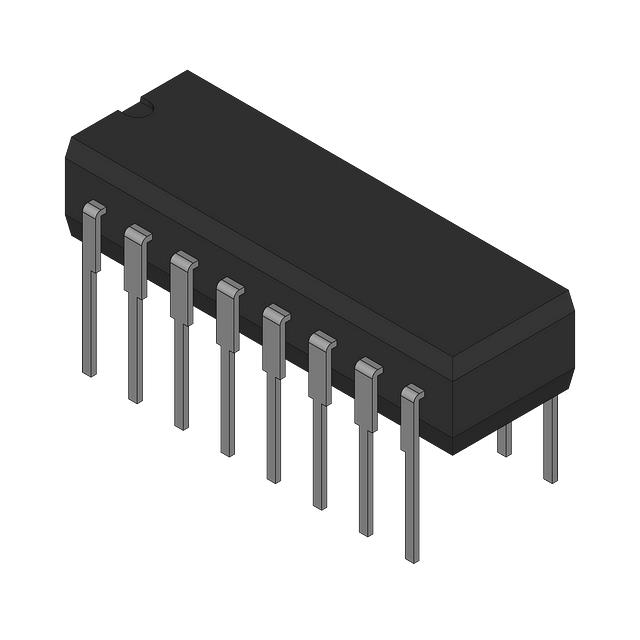
The CD54HCT367F3A is a high-speed CMOS logic device from the 54HCT series, manufactured by Texas Instruments. This product is designed to provide exceptional performance in buffering, driving, receiving, and transceiving applications. It is classified under the category of Buffers, Drivers, Receivers, and Transceivers, making it a versatile component for various electronic systems. The CD54HCT367F3A is available in bulk packaging and is currently an active product, ensuring its availability for ongoing projects and new designs. With an Export Control Classification Number (ECCN) of EAR99 and a Harmonized Tariff Schedule of the United States (HTSUS) code of 8542.39.0001, it complies with international trade regulations, facilitating seamless procurement and deployment.
CD54HCT367F3A Features
The CD54HCT367F3A boasts several key features that set it apart from similar models in the market:
- High-Speed Performance: The device operates at high speeds, ensuring efficient data transfer and minimal latency in signal processing applications. This makes it ideal for applications requiring rapid data handling and real-time processing.
- Low Power Consumption: The high-speed CMOS logic design of the CD54HCT367F3A ensures low power consumption, making it suitable for energy-sensitive applications and portable devices.
- Wide Operating Voltage Range: The device supports a wide operating voltage range, providing flexibility in system design and compatibility with various power supply configurations.
- High Noise Immunity: The CD54HCT367F3A offers high noise immunity, ensuring reliable operation in noisy environments and reducing the risk of signal corruption.
- Robust Design: The device is designed to withstand harsh operating conditions, including temperature extremes and voltage fluctuations, ensuring long-term reliability and durability.
CD54HCT367F3A Applications
The CD54HCT367F3A is well-suited for a variety of applications across different industries, including:
- Telecommunications: Ideal for buffering and driving signals in telecommunication equipment, ensuring high-speed data transmission and reliable communication.
- Automotive Electronics: Suitable for automotive applications where high-speed data processing and low power consumption are critical, such as in advanced driver-assistance systems (ADAS) and infotainment systems.
- Industrial Automation: Perfect for industrial control systems where robustness and high noise immunity are essential for reliable operation in harsh industrial environments.
- Consumer Electronics: Applicable in consumer devices requiring high-speed data handling and low power consumption, such as smartphones, tablets, and gaming consoles.
Conclusion of CD54HCT367F3A
In conclusion, the CD54HCT367F3A from Texas Instruments is a high-performance, high-speed CMOS logic device that offers significant advantages over similar models. Its low power consumption, wide operating voltage range, high noise immunity, and robust design make it an ideal choice for a wide range of applications in telecommunications, automotive electronics, industrial automation, and consumer electronics. The CD54HCT367F3A's versatility and reliability ensure that it remains a valuable component in modern electronic systems, providing efficient and dependable performance.
Tech Specifications
CD54HCT367F3A Documents
Download datasheets and manufacturer documentation for CD54HCT367F3A
Shopping Guide


.png?x-oss-process=image/format,webp/resize,h_32)


