
Texas Instruments
CD74HC112M96
Flip Flops


.png?x-oss-process=image/format,webp/resize,p_30)


CD74HC112M96 Description
CD74HC112M96 Description
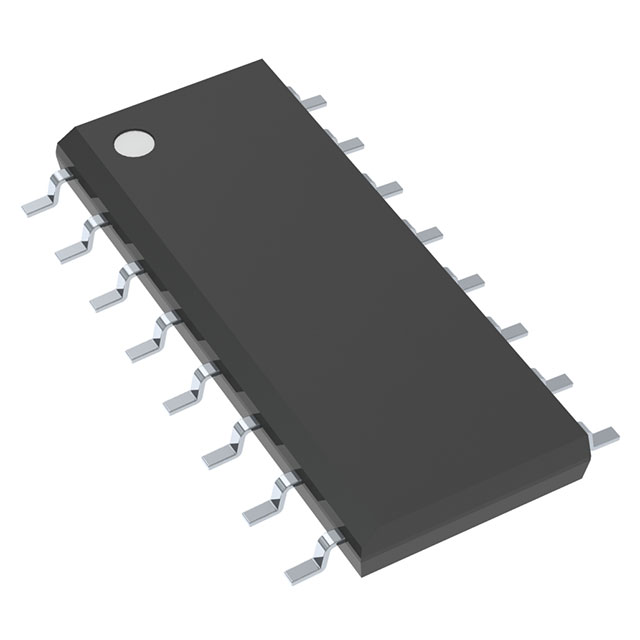
The CD74HC112M96 is a dual JK flip-flop integrated circuit (IC) designed for high-speed and reliable digital logic applications. Manufactured by Texas Instruments, this IC is part of the 74HC series, known for its high performance and compatibility with various digital systems. The CD74HC112M96 features a clock frequency of up to 60 MHz, making it suitable for high-speed digital circuits. It operates within a supply voltage range of 2V to 6V, providing flexibility in power supply requirements.
The IC is designed with complementary outputs, ensuring robust signal integrity and compatibility with a wide range of digital systems. It is triggered on the negative edge, which is beneficial for synchronous operation in digital circuits. The CD74HC112M96 also includes set (preset) and reset functions, allowing for precise control over the state of the flip-flops. Each element in the dual JK flip-flop has a single bit, making it ideal for applications requiring compact and efficient digital storage.
CD74HC112M96 Features
- High-Speed Operation: With a clock frequency of up to 60 MHz, the CD74HC112M96 ensures fast and efficient data processing, making it suitable for high-speed digital systems.
- Complementary Outputs: The complementary output type enhances signal integrity and reduces the risk of signal degradation, ensuring reliable performance in digital circuits.
- Negative Edge Triggering: The negative edge triggering mechanism allows for synchronous operation, which is crucial for maintaining the integrity of digital signals in complex systems.
- Wide Voltage Range: Operating within a supply voltage range of 2V to 6V, the CD74HC112M96 offers flexibility in power supply requirements, making it compatible with a variety of digital systems.
- Low Quiescent Current: With a quiescent current of only 4 µA, the IC is energy-efficient, making it suitable for battery-powered and low-power applications.
- High Output Current: The CD74HC112M96 can provide up to 5.2mA for both high and low outputs, ensuring strong signal drive capabilities.
- Moisture Sensitivity Level 1: The MSL 1 rating indicates that the IC is not moisture-sensitive, allowing for unlimited storage time without the need for special handling or packaging.
- Compliance and Safety: The CD74HC112M96 is REACH unaffected and RoHS3 compliant, ensuring that it meets the highest standards for environmental and safety regulations.
CD74HC112M96 Applications
The CD74HC112M96 is ideal for a wide range of digital applications, including:
- Digital Storage: The dual JK flip-flops provide compact and efficient digital storage, making the IC suitable for memory elements in digital circuits.
- Clock Management: The high-speed operation and negative edge triggering make it ideal for clock management and synchronization in digital systems.
- Signal Processing: The complementary outputs and high output current capabilities ensure reliable signal processing and transmission in digital circuits.
- Control Systems: The set (preset) and reset functions allow for precise control over the state of the flip-flops, making the IC suitable for control systems and state machines.
- Communication Systems: The wide voltage range and low quiescent current make the CD74HC112M96 suitable for communication systems where power efficiency and signal integrity are critical.
Conclusion of CD74HC112M96
The CD74HC112M96 is a versatile and high-performance dual JK flip-flop IC designed for a wide range of digital applications. Its high-speed operation, complementary outputs, and negative edge triggering make it an excellent choice for digital storage, clock management, and signal processing. The wide voltage range and low quiescent current ensure flexibility and energy efficiency, making it suitable for both high-speed and low-power applications. With its compliance with environmental and safety regulations, the CD74HC112M96 is a reliable and robust solution for modern digital systems.
Tech Specifications
CD74HC112M96 Documents
Download datasheets and manufacturer documentation for CD74HC112M96
 CD54,74HC(T)112
  CD54,74HC(T)112
  Mult Devices Font 21/Apr/2018 CDx4HC(T) 19/Oct/2022
 Shopping Guide


.png?x-oss-process=image/format,webp/resize,h_32)


