
Texas Instruments
CD74HC4052M96
Analog Switches, Multiplexers, Demultiplexers


.png?x-oss-process=image/format,webp/resize,p_30)


CD74HC4052M96 Description
CD74HC4052M96 Description
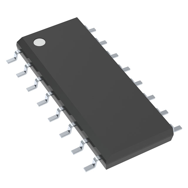
The CD74HC4052M96 is a high-performance analog switch and multiplexer/demultiplexer IC designed by Texas Instruments. This device features a 4:1 multiplexer/demultiplexer circuit with two independent SP4T (single-pole, four-throw) switch circuits. It is housed in a 16-pin SOIC package, making it suitable for surface-mount applications. The CD74HC4052M96 operates over a wide supply voltage range, from ±1V to ±5V for dual supply and from 2V to 6V for single supply, offering flexibility in various electronic designs.
CD74HC4052M96 Features
- Low On-State Resistance: The maximum on-state resistance (Ron) is 130 Ohms, ensuring minimal signal attenuation and power loss.
- High Channel-to-Channel Matching: With a ΔRon of 5 Ohms, the CD74HC4052M96 provides excellent matching between channels, crucial for applications requiring precise signal routing.
- Wide Operating Voltage Range: The device supports a dual supply voltage range of ±1V to ±5V and a single supply voltage range of 2V to 6V, making it versatile for different power supply configurations.
- Low Channel Capacitance: The channel capacitance (CS(off) and CD(off)) is only 12pF, which helps in maintaining signal integrity at high frequencies.
- High Bandwidth: The -3dB bandwidth is 185MHz, enabling the device to handle high-frequency signals efficiently.
- Low Leakage Current: The maximum leakage current (IS(off)) is 200nA, ensuring minimal power consumption and signal degradation when the switch is off.
- Compliance and Reliability: The CD74HC4052M96 is REACH unaffected and RoHS3 compliant, ensuring it meets environmental and safety standards. It also has a moisture sensitivity level (MSL) of 1, making it suitable for a wide range of manufacturing environments.
- Packaging: Available in a tape & reel (TR) package, facilitating automated assembly processes.
CD74HC4052M96 Applications
The CD74HC4052M96 is ideal for a variety of applications due to its high performance and versatility. Some specific use cases include:
- Signal Routing in Communication Systems: The low on-state resistance and high bandwidth make it suitable for routing high-frequency signals in communication systems.
- Audio and Video Switching: The device can be used in audio and video equipment to switch between different input sources, ensuring minimal signal loss and distortion.
- Test and Measurement Equipment: The precise channel matching and low leakage current are beneficial for applications requiring accurate signal measurement and switching.
- Medical Devices: The high reliability and compliance with environmental standards make it suitable for use in medical devices where precision and safety are paramount.
- Automotive Electronics: The wide operating voltage range and robustness make it ideal for automotive applications where power supply conditions can vary.
Conclusion of CD74HC4052M96
The CD74HC4052M96 from Texas Instruments is a highly versatile and reliable analog switch and multiplexer/demultiplexer IC. Its low on-state resistance, high bandwidth, and precise channel matching make it an excellent choice for applications requiring high-performance signal routing. The wide operating voltage range and compliance with environmental standards further enhance its suitability for a broad range of electronic designs. Whether used in communication systems, audio/video equipment, or medical devices, the CD74HC4052M96 offers superior performance and reliability, making it a standout choice in the market.
Tech Specifications
CD74HC4052M96 Documents
Download datasheets and manufacturer documentation for CD74HC4052M96
 CDx4HC405x, CDx4HCT405x
  CDx4HC405x, CDx4HCT405x
  Mult Devices Font 21/Apr/2018
 Shopping Guide


.png?x-oss-process=image/format,webp/resize,h_32)


