
Texas Instruments
CD74HC4052PWRG4
Analog Switches, Multiplexers, Demultiplexers


.png?x-oss-process=image/format,webp/resize,p_30)


CD74HC4052PWRG4 Description
CD74HC4052PWRG4 Description
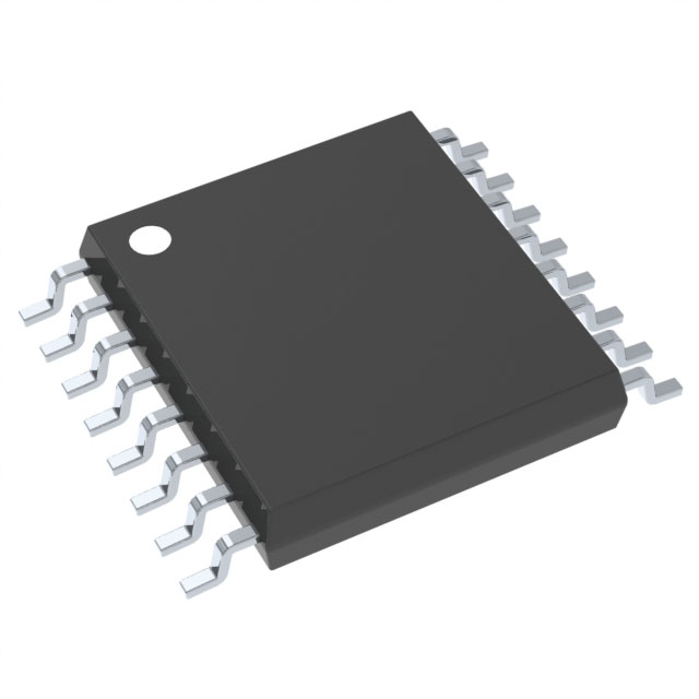
The CD74HC4052PWRG4 from Texas Instruments is a high-performance dual 4-channel analog multiplexer/demultiplexer designed for precision signal routing in mixed-signal applications. Housed in a 16-pin TSSOP package, this IC features low on-state resistance (130Ω max) and minimal channel-to-channel mismatch (ΔRon = 5Ω), ensuring consistent signal integrity. It operates across a wide voltage range (2V–6V single supply or ±1V–5V dual supply), making it versatile for both low-voltage and bipolar signal environments. With a bandwidth of 185MHz and low leakage current (200nA max), it excels in high-speed, low-power applications.
CD74HC4052PWRG4 Features
- Low On-Resistance: 130Ω max reduces signal attenuation.
- High Bandwidth: 185MHz supports high-frequency signal switching.
- Low Leakage: 200nA max ensures minimal power loss in off-state.
- Dual Supply Operation: Compatible with ±1V–5V (dual) or 2V–6V (single) supplies.
- Matched Channels: 5Ω ΔRon for uniform signal performance.
- Low Capacitance: 12pF CS(off)/CD(off) minimizes crosstalk.
- Robust Packaging: Tape & Reel (TR) 16-TSSOP for automated assembly.
- Compliance: ROHS3, REACH Unaffected, ECCN EAR99.
CD74HC4052PWRG4 Applications
- Test & Measurement: Precision signal routing in oscilloscopes and data acquisition systems.
- Audio/Video Switching: Low-distortion multiplexing in AV receivers and mixers.
- Communication Systems: Signal path selection in RF and baseband circuits.
- Industrial Control: Sensor signal conditioning and multiplexing.
- Battery-Powered Devices: Efficient signal switching in portable electronics due to low leakage.
Conclusion of CD74HC4052PWRG4
The CD74HC4052PWRG4 stands out for its low on-resistance, high bandwidth, and dual-supply flexibility, making it ideal for high-speed, low-power analog switching. While marked obsolete, its performance metrics—such as 185MHz bandwidth and 5Ω channel matching—remain competitive for legacy designs or replacements in test equipment, audio systems, and industrial controls. Engineers should evaluate alternative TI offerings for new designs but can rely on this IC for proven reliability in existing applications.
Tech Specifications
CD74HC4052PWRG4 Documents
Download datasheets and manufacturer documentation for CD74HC4052PWRG4
 CDx4HC405x, CDx4HCT405x
  OBS 21/Jun/2023
  CDx4HC405x, CDx4HCT405x
  Design 22/Feb/2022
 Shopping Guide


.png?x-oss-process=image/format,webp/resize,h_32)


