
 German
 Japanese
 Portuguese
 Korea
Korea
 Mexico
 Dutch
Dutch


Texas Instruments
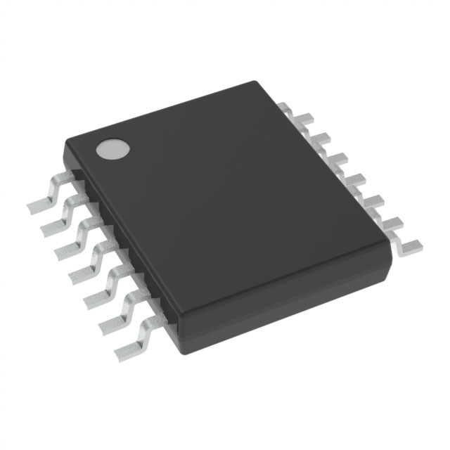
CD74HC4066PW

Why Choose Us?
Professional Platform
B2B & B2C purchasingDelivery at full speed
1-2 days deliveryWide variety
Original manufacturers365 days guarantee
Responsible quality
.png)


Tech Specifications
CD74HC4066PW Description
CD74HC4066PW Description
The CD74HC4066PW from Texas Instruments is a high-performance quad bilateral switch designed for analog signal switching in a wide range of applications. Housed in a 14-pin TSSOP package, this IC features four independent SPST (Single-Pole, Single-Throw) switches with low on-state resistance (70Ω max) and minimal leakage current (100nA max). It operates over a 2V to 10V supply range, making it compatible with both low-voltage and standard logic systems. With a -3dB bandwidth of 200MHz, it ensures high-speed signal integrity, while its low channel capacitance (5pF) minimizes signal distortion.
CD74HC4066PW Features
- Low On-State Resistance: 70Ω max ensures minimal signal attenuation.
- High Bandwidth: 200MHz supports high-frequency applications.
- Low Leakage Current: 100nA max enhances signal isolation in off-state.
- Wide Supply Range: 2V to 10V for flexibility in mixed-voltage systems.
- Low Channel Capacitance: 5pF reduces crosstalk and distortion.
- Matched Channels: ΔRon of 500mΩ ensures consistent performance across switches.
- Robust Packaging: 14-TSSOP for compact, surface-mount designs.
- Compliance: ROHS3 and REACH unaffected, suitable for environmentally conscious designs.
CD74HC4066PW Applications
- Audio/Video Signal Routing: Ideal for multimedia switches due to high bandwidth and low distortion.
- Data Acquisition Systems: Low leakage and low Ron enable precise sensor signal multiplexing.
- Communication Systems: Used in RF signal switching and modular interfaces.
- Test & Measurement Equipment: High-speed switching for automated test systems.
- Battery-Powered Devices: Low power consumption suits portable electronics.
Conclusion of CD74HC4066PW
The CD74HC4066PW stands out for its balanced performance in speed, power, and signal fidelity, making it a versatile choice for high-frequency analog switching. Its low Ron, high bandwidth, and robust packaging make it superior to generic switches, particularly in precision and high-speed applications. While it is on Last Time Buy status, its reliability and compliance ensure it remains a preferred solution for legacy and new designs requiring low-distortion signal routing.
FAQ
| Quantity | Unit Price | Ext. Price |
|---|---|---|
| 1+ | $0.94160 | $0.94 |
| 10+ | $0.67672 | $6.77 |
| 90+ | $0.54345 | $48.91 |
| 180+ | $0.51583 | $92.85 |
| 270+ | $0.50202 | $135.55 |
Not available to buy online? Want the lower wholesale price? Please Send RFQ to get best price, we will respond immediately


.png?x-oss-process=image/format,webp/resize,h_32)


