
 German
 Japanese
 Portuguese
 Korea
Korea
 Mexico
 Dutch
Dutch


Texas Instruments
CD74HC595M96

Why Choose Us?
Professional Platform
B2B & B2C purchasingDelivery at full speed
1-2 days deliveryWide variety
Original manufacturers365 days guarantee
Responsible quality
.png)


Tech Specifications
CD74HC595M96 Description
The Texas Instruments CD74HC595M96 is a high-performance, 8-bit shift register that is commonly used in digital electronics projects. Here is a description of the model, its features, and potential applications:
Description:
The CD74HC595M96 is a member of the 74HC595 family of shift registers. It is a serial-in, parallel-out 8-bit shift register that features a storage register, a transfer gate, and an output latch. The device is designed to be used in a wide range of digital electronics applications, including LED displays, digital meters, and other digital systems that require data transfer and storage.
Features:
- 8-bit serial-in, parallel-out shift register
- 3-state outputs for flexible interfacing
- Storage register and transfer gate for data transfer and storage
- Output latch for data retention
- Compatible with both TTL and CMOS logic families
- Wide operating voltage range (2V to 6V)
- Low power consumption
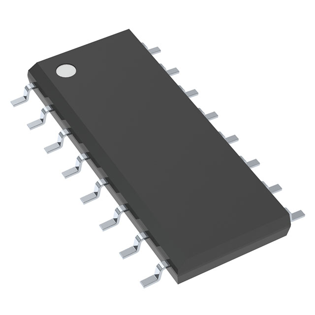
- Available in a small 16-pin SOIC package
Applications:
- LED displays: The CD74HC595M96 can be used to drive multiple LEDs in a display, allowing for efficient control and dimming of the LEDs.
- Digital meters: The shift register can be used to drive the segments of a digital meter, allowing for precise control of the displayed information.
- Data buffering: The CD74HC595M96 can be used as a buffer between a microcontroller and other digital components, providing a means to temporarily store and transfer data.
- Serial communication: The shift register can be used to interface with serial communication protocols, such as SPI or I2C, by converting parallel data to serial data and vice versa.
- Address decoding: The CD74HC595M96 can be used in memory address decoding applications, where it can store and transfer address information.
- General-purpose data transfer: The shift register can be used in various digital systems to transfer data between components, such as microcontrollers, sensors, and actuators.
In summary, the Texas Instruments CD74HC595M96 is a versatile 8-bit shift register that offers a range of features, making it suitable for a wide range of digital electronics applications. Its compact size, low power consumption, and compatibility with both TTL and CMOS logic families make it a popular choice for hobbyists and professionals alike.
FAQ
| Quantity | Unit Price | Ext. Price |
|---|---|---|
| 10+ | $0.52115 | $5.21 |
| 30+ | $0.46972 | $14.09 |
| 100+ | $0.40457 | $40.46 |
| 500+ | $0.33085 | $165.42 |
| 1000+ | $0.31372 | $313.72 |
Not available to buy online? Want the lower wholesale price? Please Send RFQ to get best price, we will respond immediately


.png?x-oss-process=image/format,webp/resize,h_32)


