
Texas Instruments
CD74HCT109M96
Flip Flops


.png?x-oss-process=image/format,webp/resize,p_30)


CD74HCT109M96 Description
CD74HCT109M96 Description
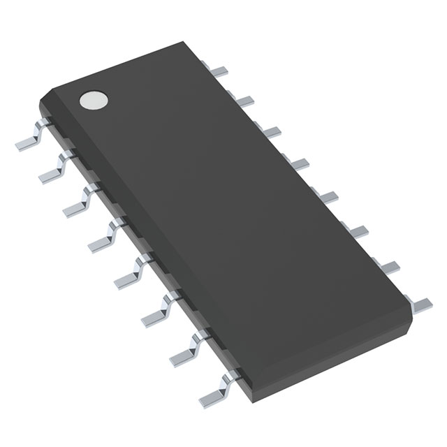
The CD74HCT109M96 is a dual JK-type flip-flop IC designed for high-speed digital applications. Manufactured by Texas Instruments, this device is part of the 74HCT series, known for its compatibility with both TTL and CMOS logic families. The CD74HCT109M96 operates within a supply voltage range of 4.5V to 5.5V and offers a maximum clock frequency of 54 MHz, making it suitable for high-speed digital circuits. Each flip-flop element supports 1-bit storage and features complementary outputs, providing flexibility in circuit design. The device is housed in a 16-pin SOIC package, which is ideal for surface-mount applications.
CD74HCT109M96 Features
- High-Speed Operation: With a maximum clock frequency of 54 MHz, the CD74HCT109M96 ensures rapid data processing and transfer, making it suitable for high-speed digital systems.
- Low Power Consumption: The device has a quiescent current of only 4 µA, which minimizes power consumption and heat generation, enhancing overall system efficiency.
- Complementary Outputs: Each flip-flop provides complementary outputs, allowing for versatile signal handling and reducing the need for additional inverters in the circuit.
- Positive Edge Triggering: The flip-flops are triggered on the positive edge of the clock signal, ensuring precise timing control and synchronization.
- Set and Reset Functionality: The CD74HCT109M96 includes set (preset) and reset functions, enabling direct control over the flip-flop states, which is crucial for initializing and managing digital circuits.
- Wide Operating Voltage Range: The device operates within a supply voltage range of 4.5V to 5.5V, providing flexibility in power supply design.
- Low Input Capacitance: With an input capacitance of 10 pF, the CD74HCT109M96 minimizes signal loading and ensures fast switching times.
- High Output Current Capability: The flip-flops can source and sink up to 4 mA, allowing them to drive a variety of digital loads without additional buffering.
- Moisture Sensitivity Level 1: The device is classified as MSL 1, meaning it is not moisture-sensitive and can be stored and handled without special precautions.
- Compliance: The CD74HCT109M96 is REACH unaffected and RoHS3 compliant, ensuring it meets environmental and safety standards.
CD74HCT109M96 Applications
The CD74HCT109M96 is ideal for a variety of digital applications, including:
- Digital Counters and Registers: The dual JK flip-flops can be used to build synchronous counters and shift registers, essential components in digital systems.
- Sequential Logic Circuits: The set and reset functions make it suitable for designing state machines and other sequential logic circuits.
- Clock Management: The positive edge triggering and high-speed operation make it ideal for clock signal management and synchronization in digital systems.
- Data Storage and Transfer: The flip-flops can be used for temporary data storage and transfer in digital circuits, ensuring reliable data handling.
- Communication Systems: The device can be used in digital communication systems for encoding, decoding, and synchronizing data signals.
Conclusion of CD74HCT109M96
The CD74HCT109M96 is a versatile and high-performance dual JK-type flip-flop IC that offers a combination of speed, low power consumption, and functional flexibility. Its high-speed operation, low input capacitance, and complementary outputs make it an excellent choice for a wide range of digital applications. The inclusion of set and reset functions, along with its compliance with environmental and safety standards, further enhances its appeal. Whether used in digital counters, sequential logic circuits, or clock management systems, the CD74HCT109M96 provides reliable performance and robust functionality, making it a valuable component in modern digital electronics.
Tech Specifications
CD74HCT109M96 Documents
Download datasheets and manufacturer documentation for CD74HCT109M96
 CD54HC(T)109, CD74HC(T)109
  Mult Devices Font 21/Apr/2018
 Shopping Guide


.png?x-oss-process=image/format,webp/resize,h_32)


