
 German
 Japanese
 Portuguese
 Korea
Korea
 Mexico
 Dutch
Dutch


Texas Instruments
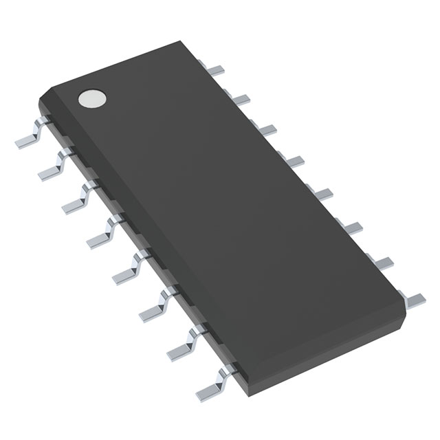
CD74HCT4053MT

Why Choose Us?
Professional Platform
B2B & B2C purchasingDelivery at full speed
1-2 days deliveryWide variety
Original manufacturers365 days guarantee
Responsible quality
.png)


Tech Specifications
CD74HCT4053MT Description
CD74HCT4053MT Description
The CD74HCT4053MT is a high-performance analog switch and multiplexer/demultiplexer IC designed by Texas Instruments. This device features a 2:1 multiplexer/demultiplexer circuit with three independent SPDT (Single Pole Double Throw) switch channels, making it highly versatile for various signal routing applications. The CD74HCT4053MT is housed in a 16-pin SOIC package, suitable for surface-mount applications, ensuring compact and reliable integration into electronic designs.
CD74HCT4053MT Features
- Low On-State Resistance: The CD74HCT4053MT boasts a maximum on-state resistance (Ron) of 130 Ohms, ensuring minimal signal attenuation and power loss, which is crucial for maintaining signal integrity in high-precision applications.
- Wide Operating Voltage Range: This IC operates within a dual supply voltage range of ±1V to ±5V and a single supply voltage range of 4.5V to 5.5V, providing flexibility in power supply options and compatibility with various system architectures.
- High Channel-to-Channel Matching: With a channel-to-channel matching (ΔRon) of 5 Ohms, the CD74HCT4053MT ensures consistent performance across all switch channels, which is essential for applications requiring precise signal routing and minimal crosstalk.
- Low Channel Capacitance: The device features low channel capacitance values of 5pF for CS(off) and 8pF for CD(off), which helps in reducing signal distortion and maintaining high-frequency performance, making it suitable for applications up to 200MHz bandwidth.
- Low Leakage Current: The maximum leakage current (IS(off)) is only 100nA, ensuring minimal power consumption and maintaining signal integrity when the switch is off.
- Compliance and Reliability: The CD74HCT4053MT is REACH unaffected and RoHS3 compliant, meeting the stringent environmental and safety standards of modern electronics. Additionally, it has a moisture sensitivity level (MSL) of 1, indicating unlimited storage conditions, which enhances its reliability and longevity.
CD74HCT4053MT Applications
The CD74HCT4053MT is ideal for a wide range of applications due to its versatile features and robust performance:
- Signal Routing in Communication Systems: The low on-state resistance and high bandwidth make it suitable for routing analog and digital signals in communication systems, ensuring minimal signal degradation.
- Audio and Video Switching: The low channel capacitance and high channel-to-channel matching are beneficial for switching audio and video signals, where signal integrity and minimal crosstalk are critical.
- Data Acquisition Systems: The device's ability to handle multiple channels with low leakage current and high matching ensures accurate signal acquisition and routing in data acquisition systems.
- Medical Equipment: The high reliability and compliance with environmental standards make it suitable for use in medical equipment where precision and safety are paramount.
Conclusion of CD74HCT4053MT
The CD74HCT4053MT from Texas Instruments stands out as a robust and versatile analog switch and multiplexer/demultiplexer IC. Its low on-state resistance, wide operating voltage range, high channel-to-channel matching, and low leakage current make it an excellent choice for applications requiring precise signal routing and minimal signal degradation. The device's compliance with environmental standards and high reliability further enhance its suitability for a wide range of applications, from communication systems to medical equipment. The CD74HCT4053MT is an ideal solution for engineers looking to integrate high-performance signal routing capabilities into their designs.
FAQ
| Quantity | Unit Price | Ext. Price |
|---|---|---|
| 1+ | $0.84480 | $0.84 |
| 10+ | $0.60368 | $6.04 |
| 25+ | $0.54490 | $13.62 |
| 100+ | $0.47960 | $47.96 |
| 250+ | $0.44845 | $112.11 |
Not available to buy online? Want the lower wholesale price? Please Send RFQ to get best price, we will respond immediately


.png?x-oss-process=image/format,webp/resize,h_32)


