
Texas Instruments
CD74HCU04QPWRQ1
Gates and Inverters


.png?x-oss-process=image/format,webp/resize,p_30)


CD74HCU04QPWRQ1 Description
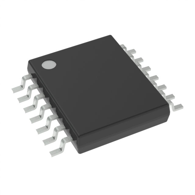
CD74HCU04QPWRQ1 is a high-performance logic inverter manufactured by Texas Instruments. It is part of the 74HCxx series of logic devices, which are known for their high-speed performance and low power consumption.
Description:
The CD74HCU04QPWRQ1 is a quad 2-input NAND gate, which means it has four independent NAND gates in a single package. Each NAND gate has two inputs and one output, and it produces a low output only when both of its inputs are high. The device is available in a surface-mount QFN package.
Features:
- High-speed performance: The CD74HCU04QPWRQ1 has a propagation delay of only 3.5 ns, making it suitable for high-speed applications.
- Low power consumption: The device has a low power consumption of only 1.2 mW per gate, which makes it ideal for battery-powered applications.
- Wide operating voltage range: The CD74HCU04QPWRQ1 can operate over a wide voltage range of 2V to 6V, making it suitable for a variety of applications.
- High noise immunity: The device has a high noise immunity of 10 kV/µs, which makes it suitable for use in noisy environments.
- Low output voltage: The device has a low output voltage of only 0.2 V, which reduces power consumption and heat generation.
Applications:
The CD74HCU04QPWRQ1 can be used in a variety of applications, including:
- Digital logic circuits: The device can be used to build digital logic circuits for a variety of applications, such as data processing, control systems, and communication systems.
- Switching circuits: The device can be used to build switching circuits for controlling the flow of power in electronic devices.
- Level shifting circuits: The device can be used to build level shifting circuits for interfacing between different voltage levels in electronic systems.
- Oscillators: The device can be used to build oscillators for generating clock signals in digital systems.
- Power management circuits: The device can be used in power management circuits for controlling the power supply to electronic devices.
In summary, the CD74HCU04QPWRQ1 is a high-performance logic inverter that offers high-speed performance, low power consumption, and a wide operating voltage range. It can be used in a variety of applications, including digital logic circuits, switching circuits, level shifting circuits, oscillators, and power management circuits.
Tech Specifications
CD74HCU04QPWRQ1 Documents
Download datasheets and manufacturer documentation for CD74HCU04QPWRQ1
 CD74HCU04Q-Q1
  CD74HCU04Q-Q1
  New Assembly Materials 02/Nov/2016 CD74HCU04-Q1 16/Jun/2020
 Shopping Guide


.png?x-oss-process=image/format,webp/resize,h_32)


