
 German
 Japanese
 Portuguese
 Korea
Korea
 Mexico
 Dutch
Dutch


Texas Instruments
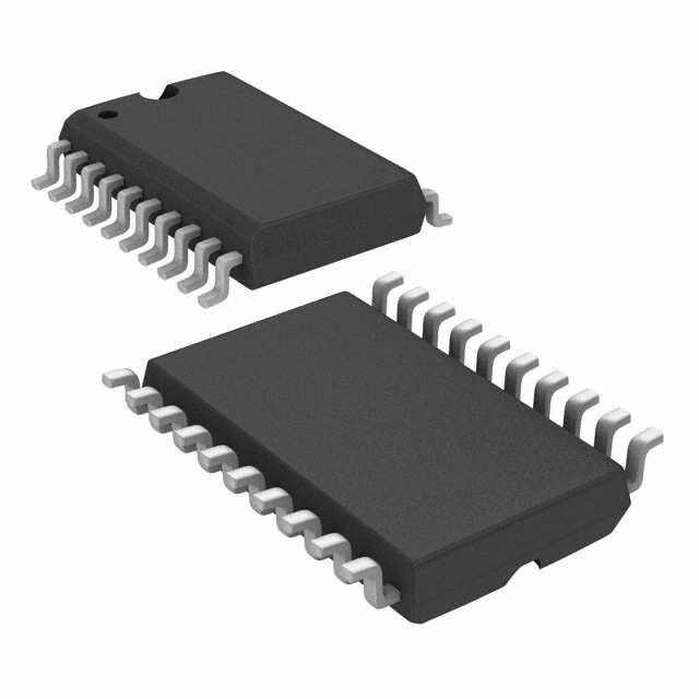
CDC204DW

Why Choose Us?
Professional Platform
B2B & B2C purchasingDelivery at full speed
1-2 days deliveryWide variety
Original manufacturers365 days guarantee
Responsible quality
.png)


Tech Specifications
CDC204DW Description
CDC204DW Description
The CDC204DW is a high-performance clock buffer/driver IC designed for a wide range of applications requiring reliable and efficient clock signal distribution. Manufactured by Texas Instruments, this device is part of the Clock/Timing ICs category and is known for its robust performance and versatility.
The CDC204DW features a 6:6 input-to-output ratio, making it ideal for applications that require multiple clock signal outputs from a single input source. It operates within a supply voltage range of 4.75V to 5.25V and can handle frequencies up to 80 MHz, ensuring compatibility with various high-speed systems. The device is designed for surface mount applications and comes in a tube package, making it suitable for automated assembly processes.
The CDC204DW is specified to operate within a temperature range of 25°C to 70°C, making it suitable for a variety of environmental conditions. It is also compliant with stringent industry standards, including REACH and RoHS3, ensuring environmental sustainability and regulatory compliance. The device has a moisture sensitivity level (MSL) of 1, indicating it is unaffected by moisture, thus enhancing its reliability in various industrial settings.
CDC204DW Features
- Operating Temperature Range: 25°C to 70°C, ensuring stable performance across a wide temperature spectrum.
- ECCN Classification: EAR99, indicating it is subject to the Export Administration Regulations (EAR) but not specifically listed in the Commerce Control List (CCL).
- Input/Output Ratio: 6:6, providing multiple output channels from a single input, ideal for clock distribution in complex systems.
- Differential Signaling: No differential signaling on both input and output, simplifying design and reducing complexity.
- Mounting Type: Surface Mount, suitable for modern, space-efficient PCB designs.
- Product Status: Active, ensuring continued availability and support from the manufacturer.
- Type: Buffer/Driver, designed to amplify and distribute clock signals efficiently.
- Input/Output Compatibility: CMOS, ensuring compatibility with a wide range of digital systems.
- Supply Voltage Range: 4.75V to 5.25V, providing flexibility in power supply options.
- Maximum Frequency: 80 MHz, suitable for high-speed clock distribution applications.
- Compliance: REACH Unaffected and ROHS3 Compliant, ensuring environmental sustainability and regulatory compliance.
- Package Type: Tube, facilitating easy handling and storage.
- Number of Circuits: 1, ensuring focused and efficient signal processing.
- HTSUS Code: 8542.39.0001, facilitating accurate customs classification and compliance.
CDC204DW Applications
The CDC204DW is well-suited for a variety of applications where reliable clock signal distribution is critical. Its high-frequency capability and multiple output channels make it ideal for:
- Telecommunications: Distributing clock signals in base stations and other communication infrastructure.
- Data Centers: Ensuring accurate clock distribution in servers and networking equipment.
- Industrial Automation: Providing stable clock signals for PLCs and other industrial control systems.
- Consumer Electronics: Enhancing the performance of high-speed digital devices such as routers and set-top boxes.
- Medical Equipment: Ensuring precise timing in diagnostic and monitoring devices.
Conclusion of CDC204DW
The CDC204DW from Texas Instruments is a versatile and reliable clock buffer/driver IC that offers a range of performance benefits and compliance features. Its 6:6 input-to-output ratio, high-frequency capability, and compatibility with CMOS signals make it an ideal choice for a variety of applications. The device's compliance with REACH and RoHS3 standards ensures it meets the highest environmental and regulatory requirements.
The CDC204DW's surface mount design and tube packaging make it suitable for modern manufacturing processes, while its wide operating temperature range and moisture sensitivity level of 1 enhance its reliability in various industrial settings. Whether used in telecommunications, data centers, industrial automation, consumer electronics, or medical equipment, the CDC204DW provides a robust solution for efficient clock signal distribution.
FAQ
| Quantity | Unit Price | Ext. Price |
|---|---|---|
| 1+ | $12.84800 | $12.85 |
| 10+ | $10.14640 | $101.46 |
| 25+ | $9.47267 | $236.82 |
| 27+ | $9.68000 | $261.36 |
| 100+ | $8.73180 | $873.18 |
Not available to buy online? Want the lower wholesale price? Please Send RFQ to get best price, we will respond immediately


.png?x-oss-process=image/format,webp/resize,h_32)


