
 German
 Japanese
 Portuguese
 Korea
Korea
 Mexico
 Dutch
Dutch


Texas Instruments
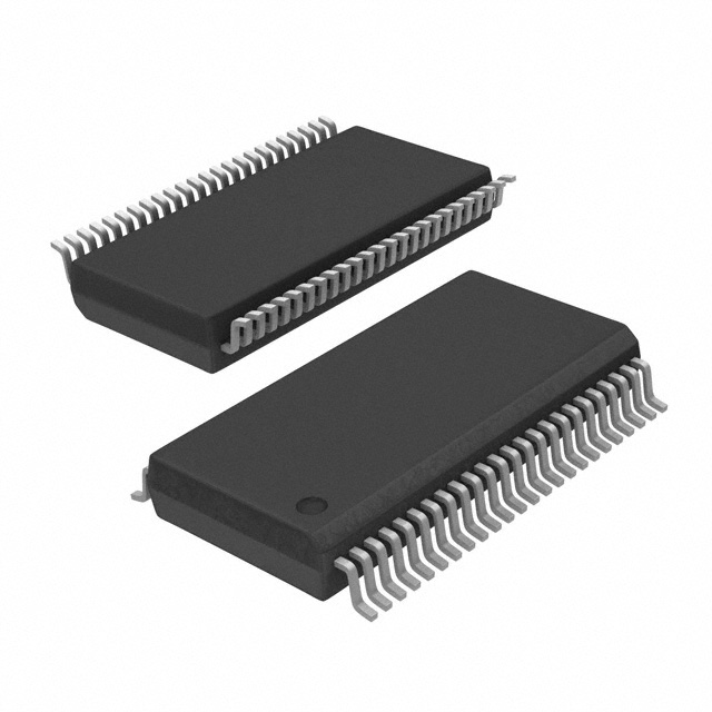
CDC318ADLR

Why Choose Us?
Professional Platform
B2B & B2C purchasingDelivery at full speed
1-2 days deliveryWide variety
Original manufacturers365 days guarantee
Responsible quality
.png)


Tech Specifications
CDC318ADLR Description
CDC318ADLR Description
The CDC318ADLR is a high-performance clock buffer designed by Texas Instruments, offering a 1:18 fanout ratio and a maximum operating frequency of 100 MHz. This device is specifically engineered for applications requiring reliable clock distribution with minimal skew and jitter. The CDC318ADLR features a single input and 18 outputs, making it ideal for distributing clock signals across multiple circuits in complex electronic systems. The input and output voltage levels are compatible with LVTTL and TTL standards, ensuring broad compatibility with various digital circuits. The device operates within a supply voltage range of 3.135V to 3.465V and is designed for surface-mount applications, providing a compact and efficient solution for modern electronics.
CDC318ADLR Features
- Operating Temperature Range: The CDC318ADLR operates reliably within a temperature range of 0°C to 70°C, making it suitable for a wide range of industrial and commercial applications.
- Fanout Ratio: With a 1:18 fanout ratio, this clock buffer can efficiently distribute clock signals to multiple destinations, reducing the need for multiple clock sources and simplifying circuit design.
- Voltage Compatibility: The device supports LVTTL input and both LVTTL and TTL output voltage levels, ensuring compatibility with a variety of digital systems.
- Supply Voltage Range: The CDC318ADLR operates within a supply voltage range of 3.135V to 3.465V, providing flexibility in power supply design.
- Surface-Mount Technology: The surface-mount package type allows for easy integration into compact and high-density PCB designs.
- High-Frequency Performance: The device supports a maximum operating frequency of 100 MHz, ensuring precise clock distribution in high-speed applications.
- Compliance and Standards: The CDC318ADLR is REACH unaffected and RoHS3 compliant, meeting stringent environmental and safety standards.
- Packaging: Available in a tape and reel package (TR), the CDC318ADLR is ideal for automated assembly processes.
CDC318ADLR Applications
The CDC318ADLR is ideal for applications requiring high-fidelity clock distribution across multiple circuits. Its 1:18 fanout ratio makes it particularly useful in systems where a single clock source needs to be distributed to numerous destinations without significant signal degradation. Some specific use cases include:
- Telecommunications: Distributing clock signals in base stations and communication equipment.
- Computing: Providing clock signals to multiple components in servers and high-performance computing systems.
- Industrial Control Systems: Ensuring precise timing in automation and control systems.
- Consumer Electronics: Enhancing the performance of multimedia devices by providing stable clock signals.
Conclusion of CDC318ADLR
The CDC318ADLR from Texas Instruments is a robust and versatile clock buffer designed to meet the demanding requirements of modern electronic systems. Its 1:18 fanout ratio, compatibility with LVTTL and TTL voltage levels, and high-frequency performance make it an excellent choice for applications requiring reliable clock distribution. The device's surface-mount package and compliance with environmental standards further enhance its suitability for a wide range of industrial and commercial applications. Whether used in telecommunications, computing, industrial control, or consumer electronics, the CDC318ADLR offers a reliable and efficient solution for clock signal distribution.
FAQ
| Quantity | Unit Price | Ext. Price |
|---|---|---|
| 1+ | $8.53600 | $8.54 |
| 10+ | $6.65632 | $66.56 |
| 25+ | $6.18534 | $154.63 |
| 43+ | $6.16880 | $265.26 |
| 100+ | $5.66764 | $566.76 |
Not available to buy online? Want the lower wholesale price? Please Send RFQ to get best price, we will respond immediately


.png?x-oss-process=image/format,webp/resize,h_32)


