
 German
 Japanese
 Portuguese
 Korea
Korea
 Mexico
 Dutch
Dutch


Texas Instruments
CDC339DW

Why Choose Us?
Professional Platform
B2B & B2C purchasingDelivery at full speed
1-2 days deliveryWide variety
Original manufacturers365 days guarantee
Responsible quality
.png)


Tech Specifications
CDC339DW Description
CDC339DW Description
The CDC339DW is a high-performance clock buffer IC designed for a wide range of electronic applications. Manufactured by Texas Instruments, this device is classified under the category of Clock Buffers and Drivers ICs. The CDC339DW features a 1:8 input-to-output ratio, making it ideal for distributing clock signals across multiple destinations with minimal signal degradation. It operates within a supply voltage range of 4.75V to 5.25V and supports TTL input and output levels, ensuring compatibility with a variety of digital systems.
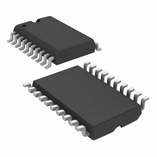
The CDC339DW is housed in a 20-pin SOIC package, which is suitable for surface mount applications, providing a compact and reliable solution for modern electronic designs. The device is rated for a maximum operating frequency of 80 MHz, making it suitable for high-speed clock distribution tasks. It is also REACH unaffected and RoHS3 compliant, ensuring environmental safety and regulatory compliance.
CDC339DW Features
- 1:8 Fanout Buffer: The CDC339DW provides a single input to eight output distribution, making it ideal for applications requiring multiple clock signals derived from a single source.
- TTL Compatibility: The device supports TTL input and output levels, ensuring seamless integration with TTL-based digital systems.
- Wide Supply Voltage Range: Operating within a supply voltage range of 4.75V to 5.25V, the CDC339DW offers flexibility in power supply requirements.
- High-Speed Performance: With a maximum operating frequency of 80 MHz, the CDC339DW is suitable for high-speed clock distribution tasks.
- Surface Mount Packaging: The 20-pin SOIC package is designed for surface mount applications, providing a compact and reliable solution for modern electronic designs.
- Environmental Compliance: The CDC339DW is REACH unaffected and RoHS3 compliant, ensuring environmental safety and regulatory compliance.
- Moisture Sensitivity Level (MSL): With an MSL rating of 1 (Unlimited), the CDC339DW is suitable for a wide range of manufacturing environments without the need for special handling.
CDC339DW Applications
The CDC339DW is ideal for a variety of applications where high-speed clock distribution is required. Some specific use cases include:
- Telecommunications: Distributing clock signals across multiple components in telecommunication equipment.
- Computing: Providing clock signals to various components within a computer system, such as CPUs, GPUs, and memory modules.
- Industrial Control Systems: Ensuring reliable clock distribution in industrial automation and control systems.
- Consumer Electronics: Distributing clock signals in devices such as televisions, gaming consoles, and other consumer electronics.
Conclusion of CDC339DW
The CDC339DW is a versatile and high-performance clock buffer IC that offers significant advantages over similar models. Its 1:8 fanout capability, wide supply voltage range, and high-speed performance make it suitable for a wide range of applications. The device's surface mount packaging and environmental compliance further enhance its appeal for modern electronic designs. Whether used in telecommunications, computing, industrial control systems, or consumer electronics, the CDC339DW provides reliable and efficient clock distribution, making it an essential component for any system requiring multiple clock signals.
FAQ
Not available to buy online? Want the lower wholesale price? Please Send RFQ to get best price, we will respond immediately


.png?x-oss-process=image/format,webp/resize,h_32)


