
 German
 Japanese
 Portuguese
 Korea
Korea
 Mexico
 Dutch
Dutch


Texas Instruments
CDC351IDB

Why Choose Us?
Professional Platform
B2B & B2C purchasingDelivery at full speed
1-2 days deliveryWide variety
Original manufacturers365 days guarantee
Responsible quality
.png)


Tech Specifications
CDC351IDB Description
CDC351IDB Description
The CDC351IDB is a high-performance clock buffer designed by Texas Instruments, specifically tailored for applications requiring precise clock signal distribution. This fanout buffer features a 1:10 input-to-output ratio, making it ideal for distributing clock signals across multiple devices with minimal signal degradation. The CDC351IDB operates within a supply voltage range of 3V to 3.6V, ensuring compatibility with a wide range of power supply configurations. It supports LVTTL input levels, providing seamless integration with existing LVTTL-based systems.
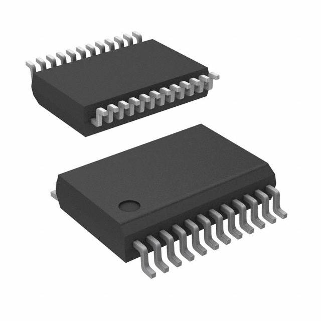
The CDC351IDB is housed in a 24-lead small outline package (SSOP) and is available in tube packaging, facilitating easy handling and integration into surface-mount designs. With a maximum operating frequency of 100 MHz, this clock buffer is well-suited for high-speed applications where signal integrity is critical. The device is REACH unaffected and RoHS3 compliant, ensuring it meets the latest environmental and safety standards.
CDC35ID1B Features
- 1:10 Fanout Buffer: Distributes a single clock signal to ten outputs, reducing the load on the original clock source and maintaining signal integrity.
- LVTTL Input Compatibility: Ensures compatibility with existing LVTTL-based systems, facilitating seamless integration.
- Wide Supply Voltage Range: Operates within a 3V to 3.6V range, providing flexibility in power supply design.
- High-Speed Performance: Capable of operating up to 100 MHz, making it suitable for high-speed clock distribution.
- Surface-Mount Compatibility: The 24-lead SSOP package is ideal for surface-mount applications, enabling compact and efficient PCB designs.
- Environmental Compliance: REACH unaffected and RoHS3 compliant, ensuring the device meets stringent environmental and safety standards.
- Moisture Sensitivity Level 1: Unlimited storage time, reducing the risk of moisture-related damage during handling and storage.
CDC351IDB Applications
The CDC351IDB is designed for a variety of applications where reliable clock signal distribution is essential. Its high-speed performance and wide supply voltage range make it suitable for:
- Telecommunications: Distributing clock signals across multiple devices in communication systems.
- Networking Equipment: Ensuring precise timing in routers, switches, and other networking hardware.
- Consumer Electronics: Providing stable clock signals in devices such as set-top boxes and gaming consoles.
- Industrial Control Systems: Maintaining accurate timing in PLCs and other industrial automation equipment.
- Medical Devices: Ensuring reliable clock distribution in medical imaging and diagnostic equipment.
Conclusion of CDC351IDB
The CDC351IDB from Texas Instruments is a robust and versatile clock buffer that excels in high-speed, high-density applications. Its 1:10 fanout capability, wide supply voltage range, and compatibility with LVTTL inputs make it a reliable choice for distributing clock signals across multiple devices. The device's environmental compliance and surface-mount compatibility further enhance its suitability for modern electronics manufacturing. Whether used in telecommunications, networking, consumer electronics, industrial control systems, or medical devices, the CDC351IDB ensures precise and reliable clock signal distribution, making it an ideal choice for engineers and designers seeking a high-performance clock buffer solution.
FAQ
| Quantity | Unit Price | Ext. Price |
|---|---|---|
| 1+ | $15.47920 | $15.48 |
| 10+ | $12.30328 | $123.03 |
| 22+ | $11.87120 | $261.17 |
| 60+ | $10.92007 | $655.20 |
| 120+ | $10.54592 | $1265.51 |
Not available to buy online? Want the lower wholesale price? Please Send RFQ to get best price, we will respond immediately


.png?x-oss-process=image/format,webp/resize,h_32)


