
 German
 Japanese
 Portuguese
 Korea
Korea
 Mexico
 Dutch
Dutch


Texas Instruments
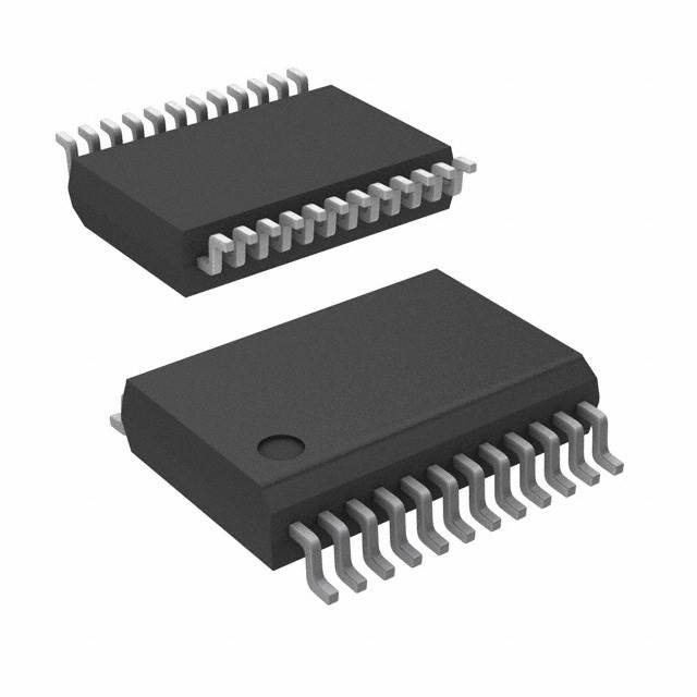
CDC351IDBG4

Why Choose Us?
Professional Platform
B2B & B2C purchasingDelivery at full speed
1-2 days deliveryWide variety
Original manufacturers365 days guarantee
Responsible quality
.png)


Tech Specifications
CDC351IDBG4 Description
CDC351IDBG4 Description
The CDC351IDBG4 is a high-performance clock buffer designed by Texas Instruments, specifically tailored for applications requiring reliable and efficient clock signal distribution. This IC features a 1:10 fanout buffer, making it ideal for distributing clock signals across multiple points in a system without significant signal degradation. The CDC351IDBG4 operates within a supply voltage range of 3V to 3.6V and supports LVTTL input levels, ensuring compatibility with a wide range of digital systems.
CDC351IDBG4 Features
- ECCN Classification: The CDC351IDBG4 is classified under ECCN EAR99, indicating its general availability and compliance with export regulations.
- Fanout Buffer: The 1:10 fanout ratio allows for efficient distribution of clock signals, reducing the need for multiple buffer stages and simplifying circuit design.
- Differential Signaling: The CDC351IDBG4 supports non-differential signaling (No/No for) both input and output, making it suitable for applications where single-ended signaling is preferred.
- Surface Mount Technology: The surface mount mounting type ensures ease of integration into modern PCB designs, enhancing reliability and reducing the footprint on the board.
- High Frequency Performance: With a maximum operating frequency of 100 MHz, the CDC351IDBG4 can handle high-speed clock signals, making it suitable for demanding applications in telecommunications, computing, and industrial electronics.
- Compliance and Safety: The CDC351IDBG4 is REACH unaffected and RoHS3 compliant, ensuring it meets the highest environmental and safety standards.
- Packaging and Availability: The device is available in a tube package, offering convenient handling and storage options for manufacturers and distributors.
- Moisture Sensitivity Level (MSL): With an MSL of 1 (Unlimited), the CDC351IDBG4 is highly resistant to moisture, reducing the risk of damage during assembly and storage.
CDC351IDBG4 Applications
The CDC351IDBG4 is ideal for a variety of applications where reliable clock signal distribution is critical. Some specific use cases include:
- Telecommunications: Distributing clock signals in base stations and communication equipment to ensure operation synchronized.
- Computing: Providing stable clock signals to various components within a computer system, such as CPUs, GPUs, and memory modules.
- Industrial Electronics: Ensuring precise timing in control systems, automation equipment, and industrial networks.
- Consumer Electronics: Enhancing the performance of devices such as routers, set-top boxes, and smart home devices by providing clean and stable clock signals.
Conclusion of CDC351IDBG4
The CDC351IDBG4 from Texas Instruments is a robust and versatile clock buffer that offers significant advantages over similar models. Its high fanout ratio, compatibility with LVTTL input levels, and ability to operate at up to 100 MHz make it a reliable choice for a wide range of applications. The device's compliance with environmental and safety standards, along with its surface mount technology and moisture resistance, further enhance its suitability for modern electronics. Whether used in telecommunications, computing, or industrial applications, the CDC351IDBG4 ensures efficient and reliable clock signal distribution, making it an essential component in high-performance electronic systems.
FAQ
Not available to buy online? Want the lower wholesale price? Please Send RFQ to get best price, we will respond immediately


![STMicroelectronics_ST232ACD_VERY HIGH SPEED, ULTRA LOW POWER CONSUMPTION 5V POWERED RS-232 DRIVERS AND RECEIVERS, [0oC, 70oC] TEMPERATURE RANGE](https://media.ersaelectronics.com/static/20240425/stmicroelectronics/74ac257mtr.jpg?x-oss-process=image/format,webp/resize,p_25)


.png?x-oss-process=image/format,webp/resize,h_32)


