

Texas Instruments
CDC391D
Clock Buffers, Drivers ICs

Not available to buy online? Want the lower wholesale price? Please Send RFQ to get best price, we will respond immediately


.png?x-oss-process=image/format,webp/resize,p_30)


CDC391D Description
CDC391D Description
The CDC391D is a high-performance clock buffer IC designed for a wide range of electronic applications requiring precise clock signal distribution. Manufactured by Texas Instruments, this device is part of the CDC391 family and is classified under Clock/Timing ICs. It features a 1:6 input-to-output ratio, making it ideal for distributing clock signals to multiple destinations without significant signal degradation. The CDC391D operates within a supply voltage range of 4.75V to 5.25V and supports TTL input and output levels, ensuring compatibility with various digital systems.
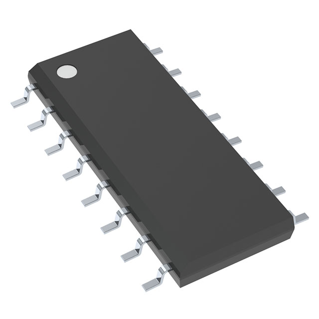
The device is housed in a surface-mount 16SOIC package, which is both compact and suitable for high-density PCB designs. With a maximum operating frequency of 100 MHz, the CDC391D ensures reliable performance in high-speed applications. Additionally, it is REACH unaffected and RoHS3 compliant, adhering to stringent environmental and safety standards. The CDC391D is available in a tube package and has a moisture sensitivity level (MSL) of 1, making it suitable for a variety of manufacturing environments.
CDC391D Features
- High Fanout Capability: The 1:6 input-to-output ratio allows the CDC391D to distribute clock signals to multiple destinations efficiently, reducing the need for multiple buffer stages.
- Wide Operating Voltage Range: The device operates within a supply voltage range of 4.75V to 5.25V, providing flexibility in power supply design.
- TTL Compatibility: Both input and output levels are TTL compatible, ensuring seamless integration with existing digital systems.
- High-Speed Performance: With a maximum operating frequency of 100 MHz, the CDC391D is suitable for high-speed clock distribution applications.
- Surface-Mount Packaging: The 16SOIC package is compact and ideal for surface-mount technology (SMT) processes, enabling high-density PCB designs.
- Environmental Compliance: The CDC391D is REACH unaffected and RoHS3 compliant, ensuring it meets environmental and safety standards.
- Moisture Sensitivity Level: MSL 1 (Unlimited) allows for flexibility in manufacturing processes without the need for special handling procedures.
CDC391D Applications
The CDC391D is well-suited for a variety of applications that require precise clock signal distribution. Some specific use cases include:
- Telecommunications: Distributing clock signals in communication systems, ensuring synchronized data transmission.
- Computing: Providing clock signals to multiple components within a computer system, such as CPUs, GPUs, and memory modules.
- Industrial Control Systems: Ensuring reliable clock distribution in industrial automation and control systems.
- Consumer Electronics: Used in devices like routers, modems, and other networking equipment to maintain accurate timing.
- Automotive Electronics: Distributing clock signals in automotive systems, such as infotainment and advanced driver-assistance systems (ADAS).
Conclusion of CDC391D
The CDC391D is a versatile and high-performance clock buffer IC that offers significant advantages over similar models. Its 1:6 fanout capability, wide operating voltage range, and TTL compatibility make it a reliable choice for various applications. The device's high-speed performance, surface-mount packaging, and environmental compliance further enhance its appeal. Whether used in telecommunications, computing, industrial control systems, consumer electronics, or automotive electronics, the CDC391D ensures precise clock signal distribution, contributing to the overall reliability and efficiency of the system.
Tech Specifications
CDC391D Documents
Download datasheets and manufacturer documentation for CDC391D
CDC391 Related Parts


Shopping Guide


.png?x-oss-process=image/format,webp/resize,h_32)


©2025 ERSA Electronics Corporation.