
 German
 Japanese
 Portuguese
 Korea
Korea
 Mexico
 Dutch
Dutch


Texas Instruments
CDC7005ZVAR

Why Choose Us?
Professional Platform
B2B & B2C purchasingDelivery at full speed
1-2 days deliveryWide variety
Original manufacturers365 days guarantee
Responsible quality
.png)


Tech Specifications
CDC7005ZVAR Description
CDC7005ZVAR Description
The CDC7005ZVAR is a high-performance clock synchronizer and jitter cleaner designed by Texas Instruments. This device is specifically engineered to provide reliable and precise clock synchronization in various electronic systems. It features a robust input and output capability, supporting LVCMOS and LVPECL input types, and LVPECL output types, making it versatile for a wide range of applications. The CDC7005ZVAR operates within a supply voltage range of 3V to 3.6V, ensuring compatibility with modern low-voltage systems.
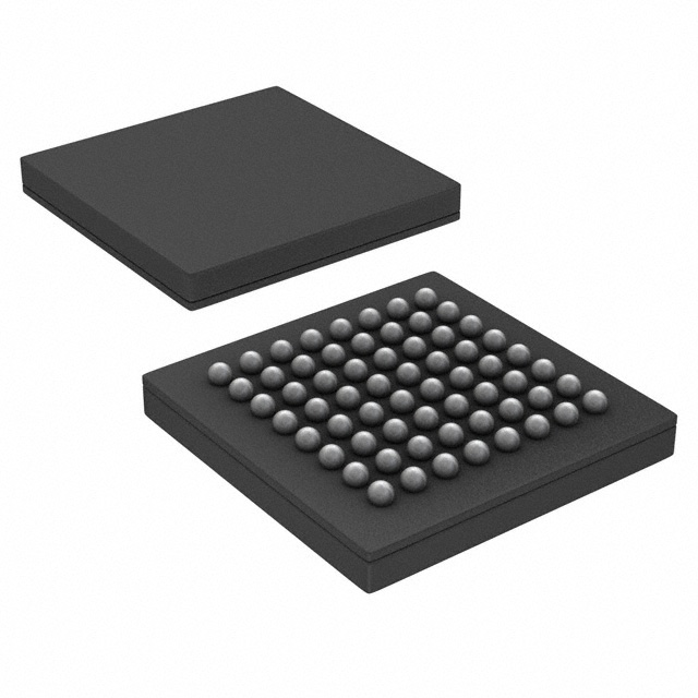
This IC is housed in a 64-ball BGA package, which is ideal for surface mount applications, offering a compact and efficient solution for space-constrained designs. The CDC7005ZVAR is designed with a 2:5 input-to-output ratio, providing flexibility in clock frequency management. It also supports differential signaling for both input and output, enhancing signal integrity and reducing electromagnetic interference (EMI).
CDC7005ZVAR Features
- Clock Synchronization and Jitter Cleaning: The CDC7005ZVAR excels in reducing jitter and maintaining signal integrity, crucial for high-speed digital systems-.
Wide Input and Output Compatibility: Supporting LVCMOS and LVPECL input types, and LVPECL output types, this IC can integrate seamlessly with various digital circuits. - Low-Voltage Operation: With a supply voltage range of 3V to 3.6V, it is well-suited for modern low-power applications.
- Flexible Frequency Management: The 2:5 input-to-output ratio allows for efficient clock frequency scaling, making it ideal for systems requiring precise clock control.
- Differential Signaling: Both input and output support differential signaling, which minimizes noise and improves signal quality.
- Surface Mount Compatibility: The 64-ball BGA package is designed for surface mount technology, ensuring ease of integration into PCB designs.
- High Maximum Frequency: Capable of operating up to 800MHz, the CDC7005ZVAR supports high-speed applications.
- Compliance and Reliability: The device is REACH unaffected Ro andHS3 compliant, ensuring environmental and regulatory standards are met. It also has a moisture sensitivity level (MSL) of 3, suitable for standard manufacturing processes.
CDC7005ZVAR Applications
The CDC7005ZVAR is ideal for a variety of applications where precise clock synchronization and low jitter are critical. Some specific use cases include:
- Telecommunications: In high-speed data transmission systems, the CDC7005ZVAR ensures reliable clock synchronization, reducing signal degradation and improving overall system performance.
- Data Centers: For server and storage systems, the CDC7005ZVAR helps maintain clock accuracy, ensuring data integrity and system reliability.
- Networking Equipment: In routers and switches, the device provides stable clock signals, enhancing the performance of high-speed data processing.
- Industrial Automation: For precision control systems, the CDC7005ZVAR ensures accurate timing, improving the efficiency and reliability of automated processes.
Conclusion of CDC7005ZVAR
The CDC7005ZVAR from Texas Instruments stands out as a reliable and high-performance clock synchronizer and jitter cleaner. Its wide range of input and output compatibility, low-voltage operation, and differential signaling capabilities make it a versatile solution for various electronic systems. The device's ability to operate up to 800MHz and its compliance with environmental and regulatory standards further enhance its appeal. For applications requiring precise clock synchronization and low jitter, the CDC7005ZVAR offers a robust and efficient solution, ensuring optimal performance and reliability.
FAQ
Not available to buy online? Want the lower wholesale price? Please Send RFQ to get best price, we will respond immediately


.png?x-oss-process=image/format,webp/resize,h_32)


