
 German
 Japanese
 Portuguese
 Korea
Korea
 Mexico
 Dutch
Dutch


Texas Instruments
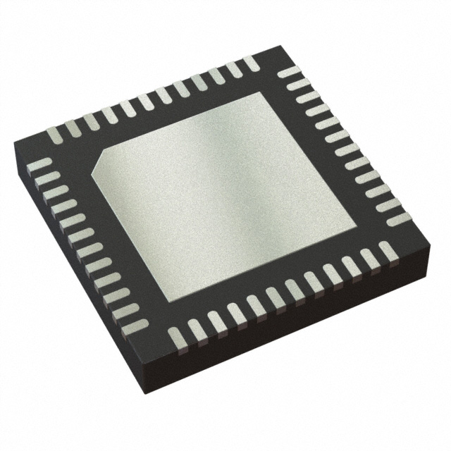
CDCDB803RSLT

Why Choose Us?
Professional Platform
B2B & B2C purchasingDelivery at full speed
1-2 days deliveryWide variety
Original manufacturers365 days guarantee
Responsible quality
.png)


Tech Specifications
CDCDB803RSLT Description
CDCDB803RSLT Description
The CDCDB803RSLT is a high-performance clock buffer designed by Texas Instruments, offering a 1:8 input-to-output ratio. This device is specifically engineered to handle high-frequency clock signals with exceptional precision and reliability. It features a differential input and output, ensuring minimal signal degradation and high noise immunity, making it ideal for demanding applications requiring high signal integrity.
CDCDB803RSLT Features
- High Frequency Performance: The CDCDB803RSLT supports a maximum frequency of 250 MHz, making it suitable for high-speed clock distribution in complex systems.
- Differential Signaling: Both the input and output are differential, which significantly reduces electromagnetic interference (EMI) and improves signal quality over long distances.
- Flexible Power Supply: The device operates within a voltage range of 3V to 3.6V, providing flexibility in power supply options and compatibility with various system designs.
- Surface Mount Technology: The surface mount package type ensures easy integration into modern PCB designs, enhancing reliability and reducing board space.
- Robust Packaging: The CDCDB803RSLT is available in a Tape & Reel (TR) package, facilitating efficient handling and assembly in high-volume manufacturing processes.
- Single Circuit Design: With a single circuit, this clock buffer is optimized for simplicity and cost-effectiveness, while maintaining high performance.
- Moisture Sensitivity Level: The MSL level of 1 (Unlimited) indicates that the device is highly resistant to moisture, ensuring long-term reliability in various environmental conditions.
CDCDB803RSLT Applications
The CDCDB803RSLT is ideal for a wide range of applications where high-frequency clock distribution is critical. Its differential signaling and high-frequency capabilities make it particularly suitable for:
- Telecommunications: In high-speed communication systems, the CDCDB803RSLT ensures precise clock distribution, minimizing timing errors and improving overall system performance.
- Data Centers: For clock distribution in servers and networking equipment, the device's high-frequency support and differential signaling enhance signal integrity and reduce latency.
- Industrial Automation: In industrial control systems, the robustness and reliability of the CDCDB803RSLT ensure accurate timing and synchronization, crucial for efficient operation.
- Consumer Electronics: In devices such as high-definition televisions and gaming consoles, the CDCDB803RSLT provides reliable clock distribution, contributing to high-quality audio and video processing.
Conclusion of CDCDB803RSLT
The CDCDB803RSLT from Texas Instruments stands out as a versatile and high-performance clock buffer, offering a 1:8 input-to-output ratio with differential signaling. Its ability to handle frequencies up to 250 MHz, combined with a flexible power supply range and robust packaging, makes it an excellent choice for a variety of applications. The device's surface mount technology and moisture resistance further enhance its reliability and ease of integration. Whether used in telecommunications, data centers, industrial automation, or consumer electronics, the CDCDB803RSLT delivers exceptional performance and reliability, making it a preferred solution for high-speed clock distribution needs.
FAQ
| Quantity | Unit Price | Ext. Price |
|---|---|---|
| 1+ | $4.20343 | $4.20 |
| 10+ | $4.10400 | $41.04 |
| 30+ | $4.03885 | $121.17 |
Not available to buy online? Want the lower wholesale price? Please Send RFQ to get best price, we will respond immediately


.png?x-oss-process=image/format,webp/resize,h_32)


