
 German
 Japanese
 Portuguese
 Korea
Korea
 Mexico
 Dutch
Dutch


Texas Instruments
CDCLVD110VF

Why Choose Us?
Professional Platform
B2B & B2C purchasingDelivery at full speed
1-2 days deliveryWide variety
Original manufacturers365 days guarantee
Responsible quality
.png)


Tech Specifications
CDCLVD110VF Description
CDCLVD110VF Description
The CDCLVD110VF is a high-performance clock buffer and multiplexer designed by Texas Instruments, specifically tailored for applications requiring reliable and efficient clock signal distribution. This IC operates with a 2:10 input-to-output ratio, making it ideal for fanout buffer and distribution applications. It features differential input and output capabilities, ensuring high signal integrity and minimal noise interference. The CDCLVD110VF is designed for surface-mount applications, offering a compact and robust solution for modern electronic designs. Despite its "Not For New Designs" status, this product remains a reliable choice for existing systems and specific use cases where its unique features are required.
CDCLVD110VF Features
- Differential Signaling: The CDCLVD110VF supports differential signaling for both input and output, which enhances signal integrity and reduces electromagnetic interference (EMI). This feature is particularly beneficial in high-speed applications where signal quality is critical.
- Wide Supply Voltage Range: The IC operates within a supply voltage range of 2.375V to 2.625V, providing flexibility in power supply design and ensuring compatibility with various power sources.
- High Frequency Performance: With a maximum operating frequency of 1.1 GHz, the CDCLVD110VF is capable of handling high-speed clock signals, making it suitable for advanced electronic systems that require precise timing and synchronization.
- Compliance and Standards: The CDCLVD110VF meets important industry standards, including REACH Unaffected and ROHS3 compliance, ensuring it is environmentally friendly and suitable for use in a wide range of applications.
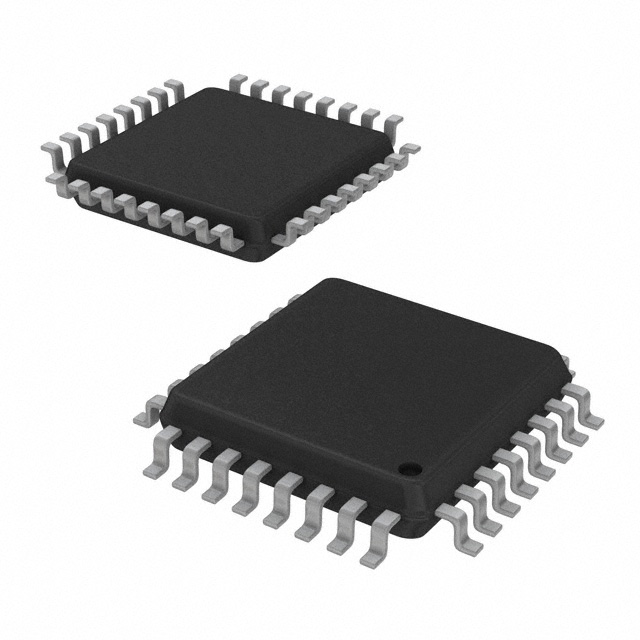
- Packaging and Mounting: The IC is available in a 32LQFP package and is designed for surface-mount technology (SMT), which simplifies assembly processes and enhances the reliability of the final product.
- Moisture Sensitivity Level: With an MSL rating of 1 (Unlimited), the CDCLVD110VF is highly resistant to moisture, making it suitable for use in various environmental conditions without the need for special handling or storage requirements.
CDCLVD110VF Applications
The CDCLVD110VF is well-suited for a variety of applications, particularly those that require high-speed clock signal distribution and multiplexing. Some specific use cases include:
- Telecommunications: In high-speed communication systems, the CDCLVD110VF can be used to distribute clock signals across multiple components, ensuring precise timing and synchronization.
- Data Centers: For managing clock signals in server racks and data processing units, the IC's differential signaling and high-frequency capabilities make it an ideal choice.
- Industrial Automation: In environments where reliability and signal integrity are paramount, the CDCLVD110VF can be used to distribute clock signals to various control units and sensors.
- Medical Equipment: For medical imaging and diagnostic devices that require precise timing and high-speed data processing, the CDCLVD110VF ensures reliable clock signal distribution.
Conclusion of CDCLVD110VF
The CDCLVD110VF from Texas Instruments is a versatile and high-performance clock buffer and multiplexer that offers significant advantages in terms of signal integrity, frequency performance, and compliance with industry standards. Although it is not recommended for new designs, its unique features and robust performance make it an excellent choice for existing systems and specific applications where its capabilities are essential. The combination of differential signaling, wide supply voltage range, and high-frequency operation ensures that the CDCLVD110VF remains a reliable and efficient solution for clock signal distribution and multiplexing in various electronic systems.
FAQ
Not available to buy online? Want the lower wholesale price? Please Send RFQ to get best price, we will respond immediately


.png?x-oss-process=image/format,webp/resize,h_32)


