
 German
 Japanese
 Portuguese
 Korea
Korea
 Mexico
 Dutch
Dutch


Texas Instruments
CDCLVD110VFR

Why Choose Us?
Professional Platform
B2B & B2C purchasingDelivery at full speed
1-2 days deliveryWide variety
Original manufacturers365 days guarantee
Responsible quality
.png)


Tech Specifications
CDCLVD110VFR Description
CDCLVD110VFR Description
The CDCLVD110VFR is a-performance high clock buffer and multiplexer designed by Texas Instruments, specifically tailored for applications requiring precise clock distribution and signal integrity. This device features a 2:10 input-to-output ratio, enabling efficient fanout of clock signals across multiple channels. The CDCLVD110VFR supports LVDS (Low-Voltage Differential Signaling) both at the input and output stages, ensuring robust signal transmission with minimal noise and interference. It operates within a supply voltage range of 2.375V to 2.625V, making it suitable for low-power applications while maintaining high performance.
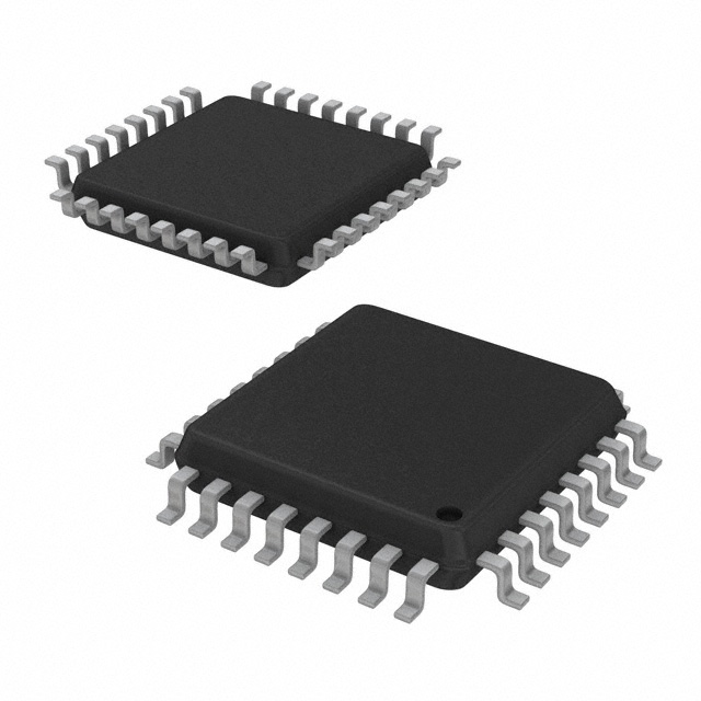
The CDCLVD110VFR is housed in a 32LQFP package and is available in a surface-mount configuration, facilitating easy integration into compact and high-density PCB designs. Despite its small form factor, it boasts a maximum operating frequency of 1.1 GHz, ensuring it can handle high-speed clock signals with ease. This device is REACH unaffected and RoHS3 compliant, adhering to stringent environmental and safety standards. Additionally, it has a moisture sensitivity level (MSL) of 1 (unlimited), making it highly durable and suitable for a wide range of operating conditions.
CDCLVD110VFR Features
- High-Speed Performance: With a maximum operating frequency of 1.1 GHz, the CDCLVD110VFR is designed to handle high-speed clock signals, making it ideal for demanding applications such as high-speed data communication and advanced computing systems.
- LVDS Compatibility: The device supports LVDS for both input and output, ensuring high signal integrity and reduced electromagnetic interference (EMI). This feature is particularly beneficial in applications where signal quality and noise reduction are critical.
- Efficient Fanout: The 2:10 input-to-output ratio allows for efficient distribution of clock signals across multiple channels, simplifying clock tree design and reducing the need for additional components.
- Low-Power Operation: Operating within a supply voltage range of 2.375V to 2.625V, the CDCLVD110VFR is optimized for low-power consumption, making it suitable for energy-efficient designs.
- Surface-Mount Packaging: The surface-mount configuration and 32LQFP package make the device easy to integrate into compact and high-density PCB designs, enhancing overall system compactness and reliability.
- Environmental Compliance: The CDCLVD110VFR is REACH unaffected and RoHS3 compliant, ensuring it meets the highest environmental and safety standards, making it suitable for global deployment.
- Durability: With an MSL of 1 (unlimited), the is device highly durable and can withstand a wide range of operating conditions, ensuring long-term reliability and performance.
CDCLVD110VFR Applications
The CDCLVD110VFR is ideal for a variety of applications where high-speed clock distribution and signal integrity are paramount. Some specific use cases include:
- High-Speed Data Communication Systems: The device's high-frequency capabilities and LVDS compatibility make it suitable for applications such as Ethernet switches, routers, and other high data-speed transmission systems.
- Advanced Computing Systems: In high-performance computing environments, the CDCLVD110VFR can efficiently distribute clock signals across multiple processing units, ensuring synchronized operation and optimal performance.
-Telecommunications Infrastructure: The device's robust signal integrity and low-power operation make it ideal for use in telecommunication equipment, such as base stations and optical networking devices. - Industrial Automation: The CDCLVD11V0FR's durability and environmental compliance make it suitable for industrial applications where reliability and long-term performance are critical.
Conclusion of CDCLVD110VFR
The CDCLVD110VFR from Texas Instruments is a versatile and high-performance clock buffer and multiplexer, offering a unique combination of high-speed operation, LVDS compatibility, and efficient fanout capabilities. Its low-power design, surface-mount packaging, and environmental compliance make it a reliable choice for a wide of range applications. While it is marked as "Not For New Designs," the CDCLVD110VFR remains a valuable component for existing systems and legacy designs, ensuring continued performance and reliability.
FAQ
Not available to buy online? Want the lower wholesale price? Please Send RFQ to get best price, we will respond immediately


.png?x-oss-process=image/format,webp/resize,h_32)


