

Texas Instruments
CDCLVD2104RHDT
Clock Buffers, Drivers ICs

Not available to buy online? Want the lower wholesale price? Please Send RFQ to get best price, we will respond immediately


.png?x-oss-process=image/format,webp/resize,p_30)


CDCLVD2104RHDT Description
CDCLVD2104RHDT Description
The CDCLVD2104RHDT is a high-performance clock buffer designed by Texas Instruments, specifically tailored for applications requiring precise clock distribution and signal integrity. This device features a 1:4 fanout ratio, enabling it to distribute a single input clock signal to four output signals with minimal skew and jitter. The CDCLVD2104RHDT operates within a supply voltage range of 2.375V to 2.625V and supports a maximum frequency of 800 MHz, making it suitable for high-speed digital systems.
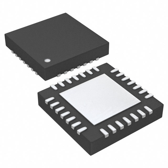
The device is designed with differential signaling, supporting both LVDS (Low Voltage Differential Signaling) and LVPECL (Low Voltage Positive Emitter-Coupled Logic) inputs and LVDS outputs. This ensures robust signal integrity and noise immunity, which is crucial for high-frequency applications. The CDCLVD2104RHDT is packaged in a 28-pin VQFN (VQFN) surface-mount package, which is ideal for compact, high-density designs.
CDCLVD2104RHDT Features
- High Fanout Capability: The 1:4 fanout ratio allows for efficient distribution of clock signals across multiple circuits, reducing the need for multiple clock sources and simplifying system design.
- Wide Input Compatibility: Supports LVCMOS, LVDS, and LVPECL input signals, providing flexibility in interfacing with various types of clock sources.
- High-Speed Performance: Capable of operating up to 800 MHz, ensuring it meets the demands of high-speed digital systems.
- Differential Signaling: Both input and output are differential, which minimizes electromagnetic interference (EMI) and improves signal integrity.
- Surface-Mount Packaging: The 28-pin VQFN package is ideal for surface-mount technology (SMT) processes, enabling compact and reliable board designs.
- Compliance and Reliability: The CDCLVD2104RHDT is REACH unaffected and RoHS3 compliant, ensuring it meets environmental and safety standards. Additionally, it has a moisture sensitivity level (MSL) of 2 (1 Year), making it suitable for a wide range of manufacturing environments.
CDCLVD2104RHDT Applications
The CDCLVD2104RHDT is ideal for a variety of applications where high-speed clock distribution and signal integrity are critical. Some specific use cases include:
- Telecommunications: In high-speed communication systems, the CDCLVD2104RHDT can distribute clock signals to multiple transceivers, ensuring synchronized data transmission and reception.
- Data Centers: For server and storage systems, the device can provide reliable clock distribution to multiple processing units, maintaining system performance and data integrity.
- Industrial Automation: In industrial control systems, the CDCLVD2104RHDT can distribute clock signals to various modules, ensuring precise timing and synchronization.
- Consumer Electronics: In high-definition video processing and display systems, the device can distribute clock signals to multiple processing units, ensuring synchronized video and audio output.
Conclusion of CDCLVD2104RHDT
The CDCLVD2104RHDT from Texas Instruments is a versatile and high-performance clock buffer that excels in applications requiring precise clock distribution and signal integrity. Its wide input compatibility, high-speed performance, and differential signaling make it a reliable choice for a variety of high-speed digital systems. The surface-mount packaging and compliance with environmental and safety standards further enhance its suitability for modern electronics manufacturing. Whether in telecommunications, data centers, industrial automation, or consumer electronics, the CDCLVD2104RHDT stands out as a robust and efficient solution for clock distribution needs.
Tech Specifications
CDCLVD2104RHDT Documents
Download datasheets and manufacturer documentation for CDCLVD2104RHDT
Wafer Fab Site 02/Dec/2022 CDCLVD2104 CDCLVD2104 Mult Dev Material Chg 29/Mar/2018 Related Parts


Shopping Guide


.png?x-oss-process=image/format,webp/resize,h_32)


©2025 ERSA Electronics Corporation.