
 German
 Japanese
 Portuguese
 Korea
Korea
 Mexico
 Dutch
Dutch


Texas Instruments
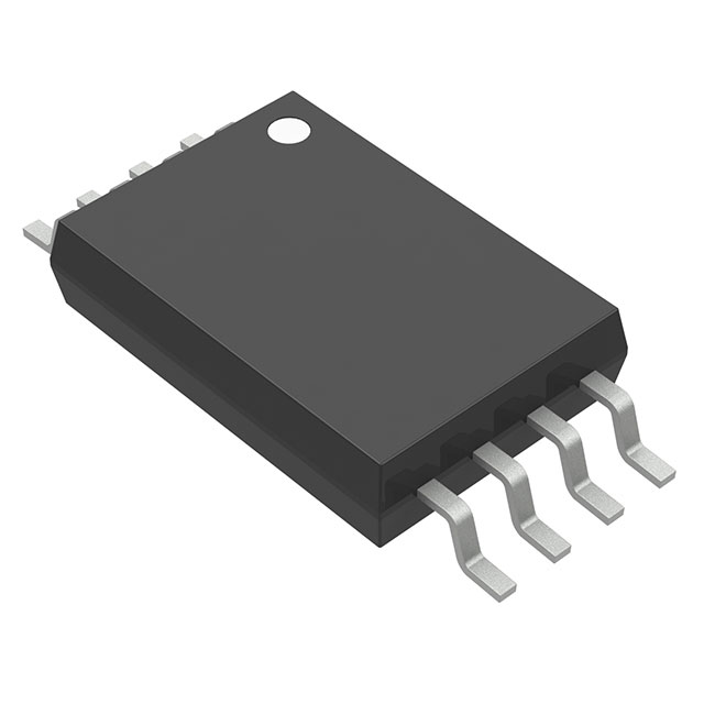
CDCS502PWR

Why Choose Us?
Professional Platform
B2B & B2C purchasingDelivery at full speed
1-2 days deliveryWide variety
Original manufacturers365 days guarantee
Responsible quality
.png)


Tech Specifications
CDCS502PWR Description
CDCS502PWR Description
The CDCS502PWR is a high-performance Spread Spectrum Clock Driver designed and manufactured by Texas Instruments. This IC is specifically engineered to provide reliable and precise clock generation and distribution in various electronic systems. With a maximum frequency of 108MHz and a 1:1 input-to-output ratio, the CDCS502PWR is well-suited for applications requiring high-speed clock signals. Its LVCMOS output and 3V to 3.6V supply voltage make it compatible with a wide range of devices.
CDCS502PWR Features
- Spread Spectrum Clock Driver: The CDCS502PWR is designed to minimize electromagnetic interference (EMI) by spreading the clock signal's frequency spectrum. This feature is particularly beneficial in applications where EMI is a concern, such as in communication systems and high-speed data processing equipment.
- Crystal Input: The CDCS502PWR accepts a crystal input, providing a stable and accurate clock source.
- LVCMOS Output: The LVCMOS output interface is widely used in digital systems, making the CDCS502PWR compatible with various downstream devices.
- Voltage - Supply: The 3V to 3.6V supply voltage range ensures compatibility with low-voltage systems.
- REACH Unaffected: The CDCS502PWR is not affected by the Registration, Evaluation, Authorization, and Restriction of Chemicals (REACH) regulations, ensuring compliance with European Union environmental standards.
- RoHS3 Compliant: The CDCS502PWR adheres to the Restriction of Hazardous Substances Directive, making it suitable for use in environmentally conscious applications.
- Moisture Sensitivity Level (MSL) 1: With an MSL of 1, the CDCS502PWR can be stored and handled without special precautions, simplifying logistics and manufacturing processes.
CDCS502PWR Applications
The CDCS502PWR is ideal for a variety of applications where high-speed, stable clock signals are required:
- Communication Systems: In wireless and wired communication systems, the CDCS502PWR can provide the necessary clock signals for data transmission and processing.
- High-Speed Data Processing: For applications such as servers and high-performance computing, the CDCS502PWR ensures stable and accurate clock signals for data processing tasks.
- Automotive Electronics: In automotive systems, the CDCS502PWR can provide reliable clock signals for infotainment systems, sensor processing, and control units.
Conclusion of CDCS502PWR
The CDCS502PWR from Texas Instruments is a versatile and high-performance Spread Spectrum Clock Driver. Its unique features, such as spread spectrum technology and compatibility with a wide range of input and output interfaces, make it an ideal choice for applications requiring high-speed and stable clock signals. With its compliance with environmental regulations and ease of handling, the CDCS502PWR is a reliable solution for a variety of electronic systems.
FAQ
Not available to buy online? Want the lower wholesale price? Please Send RFQ to get best price, we will respond immediately


.png?x-oss-process=image/format,webp/resize,h_32)


