
 German
 Japanese
 Portuguese
 Korea
Korea
 Mexico
 Dutch
Dutch



Texas Instruments
CDCV857ADGG


Why Choose Us?
Professional Platform
B2B & B2C purchasingDelivery at full speed
1-2 days deliveryWide variety
Original manufacturers365 days guarantee
Responsible quality

.png)



Tech Specifications
CDCV857ADGG Description
CDCV857ADGG Description
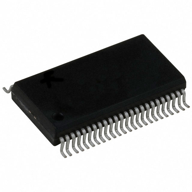
The CDCV857ADGG is a high-performance PLL clock driver designed by Texas Instruments, suitable for a wide range of applications requiring precise clock signal generation and distribution. This device is housed in a 48-TSSOP package, making it ideal for surface mount applications. The CDCV857ADGG operates within a supply voltage range of 2.3V to 2.7V and is capable of handling input and output clock signals. It features a PLL with bypass functionality, allowing for flexible clock management and ensuring high signal integrity.
The CDCV857ADGG supports a maximum frequency of 180MHz, making it suitable for high-speed applications. It has a 1:10 input-to-output ratio, which is ideal for applications requiring signal multiplication. The device also supports differential signaling for both input and output, enhancing signal quality and reducing electromagnetic interference (EMI). With a moisture sensitivity level (MSL) of 2 (1 Year), the CDCV857ADGG is well-suited for environments where moisture resistance is important.
CDCV857ADGG Features
- PLL with Bypass: The CDCV857ADGG features a Phase-Locked Loop (PLL) with bypass functionality, allowing for flexible clock management and ensuring high signal integrity.
- High-Speed Operation: Capable of operating at a maximum frequency of 180MHz, making it suitable for high-speed applications.
- Differential Signaling: Supports differential signaling for both input and output, enhancing signal quality and reducing EMI.
- Wide Supply Voltage Range: Operates within a supply voltage range of 2.3V to 2.7V, providing flexibility in power supply design.
- 1:10 Input-to-Output Ratio: Ideal for applications requiring signal multiplication.
- Moisture Sensitivity Level 2 (1 Year): Suitable for environments where moisture resistance is important.
- Surface Mount Packaging: Housed in a 48-TSSOP package, making it ideal for surface mount applications.
- Compliance: REACH unaffected and ROHS3 compliant, ensuring environmental and regulatory standards are met.
CDCV857ADGG Applications
The CDCV857ADGG is well-suited for a variety of applications where precise clock signal generation and distribution are critical. Some specific use cases include:
- Telecommunications: Ideal for applications requiring high-speed clock distribution, such as in base stations and network equipment.
- Data Centers: Useful for managing clock signals in servers and storage systems, ensuring reliable data processing and transmission.
- Industrial Automation: Suitable for applications where precise timing and synchronization are required, such as in control systems and robotics.
- Medical Equipment: Can be used in medical imaging and diagnostic devices where accurate clock signals are essential for performance.
Conclusion of CDCV857ADGG
The CDCV857ADGG from Texas Instruments is a robust PLL clock driver designed for high-speed applications requiring precise clock signal generation and distribution. Its features, such as the PLL with bypass, differential signaling, and wide supply voltage range, make it a versatile and reliable choice. The device's compliance with REACH and ROHS3 standards ensures it meets environmental and regulatory requirements. While it is not recommended for new designs, the CDCV857ADGG remains a valuable component for existing systems and applications where its unique features and performance benefits are required.
FAQ
Not available to buy online? Want the lower wholesale price? Please Send RFQ to get best price, we will respond immediately












.png?x-oss-process=image/format,webp/resize,h_32)


