
 German
 Japanese
 Portuguese
 Korea
Korea
 Mexico
 Dutch
Dutch


Texas Instruments
CDCVF2310MPWREP

Why Choose Us?
Professional Platform
B2B & B2C purchasingDelivery at full speed
1-2 days deliveryWide variety
Original manufacturers365 days guarantee
Responsible quality
.png)


Tech Specifications
CDCVF2310MPWREP Description
CDCVF2310MPWREP Description
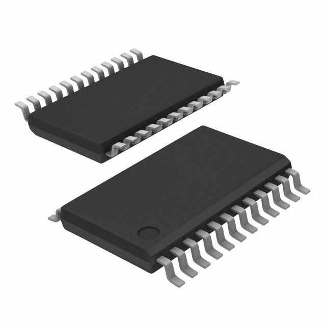
The CDCVF2310MPWREP is a high-performance Fanout Buffer (Distribution) IC designed by Texas Instruments, ideal for applications requiring reliable clock signal distribution. This device features a 1:10 input-to-output ratio, making it suitable for efficiently distributing clock signals across multiple channels. The CDCVF2310MPWREP operates with LVTTL input and output levels, ensuring compatibility with a wide range of digital systems. It supports a supply voltage range of 2.3V to 3.6V, providing flexibility in power supply design. With a maximum operating frequency of 200 MHz, this IC is well-suited for high-speed clock distribution in various electronic systems.
CDCVF2310MPWREP Features
- High-Speed Performance: The CDCVF2310MPWREP supports a maximum frequency of 200 MHz, ensuring precise and reliable clock signal distribution even in high-speed applications.
- LVTTL Compatibility: The device is designed to work with LVTTL input and output levels, making it compatible with a broad range of digital circuits.
- Flexible Power Supply: With a supply voltage range of 2.3V to 3.6V, the CDCVF2310MPWREP offers flexibility in power supply design, accommodating various power requirements.
- Surface Mount Technology: The surface mount package type facilitates easy integration into compact and high-density PCB designs.
- Compliance and Reliability: The CDCVF2310MPWREP is REACH Unaffected and RoHS3 Compliant, ensuring it meets stringent environmental and safety standards. It also has a Moisture Sensitivity Level (MSL) of 1 (Unlimited), making it suitable for a wide range of manufacturing environments.
- Packaging: Available in Tape & Reel (TR) packaging, the CDCVF2310MPWREP is ideal for automated assembly processes, enhancing production efficiency.
CDCVF2310MPWREP Applications
The CDCVF2310MPWREP is designed for a variety of applications where reliable clock signal distribution is critical. Its high-speed performance and LVTTL compatibility make it suitable for:
- Telecommunications: Distributing clock signals in high-speed communication systems, ensuring synchronization and data integrity.
- Computing: Enhancing the performance of multi-core processors and high-speed memory systems by providing stable clock signals.
- Industrial Control Systems: Ensuring precise timing and synchronization in complex industrial automation and control systems.
- Consumer Electronics: Improving the reliability and performance of digital devices such as routers, switches, and high-speed interfaces.
Conclusion of CDCVF2310MPWREP
The CDCVF2310MPWREP from Texas Instruments is a robust and versatile Fanout Buffer (Distribution) IC designed to meet the demanding requirements of modern electronic systems. Its high-speed performance, LVTTL compatibility, and flexible power supply options make it an ideal choice for a wide range of applications. The device's compliance with environmental and safety standards, along with its surface mount package, ensures ease of integration and reliability in various manufacturing processes. Whether used in telecommunications, computing, industrial control systems, or consumer electronics, the CDCVF2310MPWREP delivers exceptional performance and reliability, making it a standout choice in the market.
FAQ
| Quantity | Unit Price | Ext. Price |
|---|---|---|
| 1+ | $16.48285 | $16.48 |
| 10+ | $15.94800 | $159.48 |
Not available to buy online? Want the lower wholesale price? Please Send RFQ to get best price, we will respond immediately


.png?x-oss-process=image/format,webp/resize,h_32)


