
 German
 Japanese
 Portuguese
 Korea
Korea
 Mexico
 Dutch
Dutch


Texas Instruments
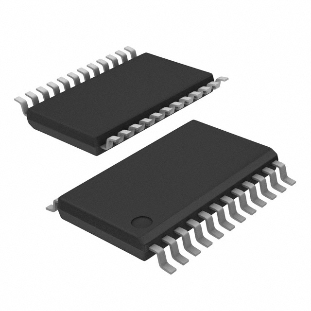
CDCVF2310PW

Why Choose Us?
Professional Platform
B2B & B2C purchasingDelivery at full speed
1-2 days deliveryWide variety
Original manufacturers365 days guarantee
Responsible quality
.png)


Tech Specifications
CDCVF2310PW Description
CDCVF2310PW Description
The CDCVF2310PW is a high-performance fanout buffer (distribution) IC manufactured by Texas Instruments. It is designed to provide a 1:10 input-output ratio, making it ideal for applications requiring signal distribution and amplification. This device operates over a wide voltage supply range of 2.3V to 3.6V and supports LVTTL input and output levels. The CDCVF2310PW is RoHS3 compliant, REACH unaffected, and has an ECCN classification of EAR99.
CDCVF2310PW Features
- Type: Fanout Buffer (Distribution)
- Ratio - Input:Output: 1:10
- Differential - Input:Output: No/No
- Mounting Type: Surface Mount
- Product Status: Active
- Input: LVTTL
- Output: LVTTL
- Voltage - Supply: 2.3V ~ 3.6V
- Frequency - Max: 200 MHz
- RoHS Status: ROHS3 Compliant
- REACH Status: REACH Unaffected
- ECCN: EAR99
- HTSUS: 8542.39.0001
- Package: Tube
- Number of Circuits: 1
- Base Product Number: CDCVF2310
- Moisture Sensitivity Level (MSL): 1 (Unlimited)
CDCVF2310PW Applications
The CDCVF2310PW is well-suited for a variety of applications where signal distribution and amplification are required. Some specific use cases include:
- Clock Buffering: The device's ability to handle LVTTL input and output levels makes it ideal for clock buffering applications in digital systems.
- Signal Distribution: The 1:10 input-output ratio allows for efficient signal distribution in complex electronic systems.
- Amplification: The CDCVF2310PW can be used to amplify signals in various applications, such as communication systems and data transmission.
- Surface Mount Technology: The surface mount packaging allows for easy integration into PCB designs, making it suitable for high-density applications.
Conclusion of CDCVF2310PW
The CDCVF2310PW is a versatile fanout buffer (distribution) IC that offers a combination of high performance, wide voltage supply range, and low power consumption. Its 1:10 input-output ratio and LVTTL support make it an ideal choice for clock buffering, signal distribution, and amplification applications. With its RoHS3 compliance, REACH unaffected status, and surface mount packaging, the CDCVF2310PW is a reliable and efficient solution for a wide range of electronic systems.
FAQ
| Quantity | Unit Price | Ext. Price |
|---|---|---|
| 1+ | $5.68972 | $5.69 |
Not available to buy online? Want the lower wholesale price? Please Send RFQ to get best price, we will respond immediately


.png?x-oss-process=image/format,webp/resize,h_32)


