
 German
 Japanese
 Portuguese
 Korea
Korea
 Mexico
 Dutch
Dutch


Texas Instruments
CDCVF2310PWRG4

Why Choose Us?
Professional Platform
B2B & B2C purchasingDelivery at full speed
1-2 days deliveryWide variety
Original manufacturers365 days guarantee
Responsible quality
.png)


Tech Specifications
CDCVF2310PWRG4 Description
CDCVF2310PWRG4 Description
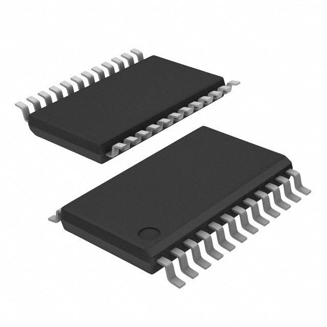
The CDCVF2310PWRG4 from Texas Instruments is a high-performance 1:10 LVTTL fanout buffer designed for precise clock distribution in demanding electronic systems. Operating within a 2.3V to 3.6V supply range, this surface-mount IC delivers robust signal integrity with a maximum frequency of 200 MHz, making it ideal for applications requiring low-jitter, high-fanout clock distribution. Its non-differential input/output architecture simplifies integration while maintaining compatibility with LVTTL logic levels. Packaged in a 24-pin TSSOP and available in tape-and-reel (TR) format, it supports automated assembly processes. The device is RoHS3 compliant, REACH unaffected, and rated for MSL 1 (unlimited) moisture sensitivity, ensuring reliability in industrial and commercial environments.
CDCVF2310PWRG4 Features
- 1:10 Clock Distribution: Provides high-fanout capability with minimal skew for synchronized system timing.
- Wide Voltage Range (2.3V–3.6V): Compatible with low-voltage designs and battery-powered applications.
- LVTTL I/O: Ensures seamless interfacing with standard logic families.
- 200 MHz Maximum Frequency: Supports high-speed clocking for processors, FPGAs, and communication interfaces.
- Surface-Mount (TSSOP-24): Compact footprint suitable for space-constrained PCBs.
- Industrial Robustness: RoHS3 compliance, REACH exemption, and MSL1 rating enhance durability.
- Low Jitter: Optimized for applications demanding precise timing, such as networking and data acquisition.
CDCVF2310PWRG4 Applications
This buffer excels in systems requiring high-fanout, low-skew clock distribution, including:
- Telecommunications: Synchronizing baseband processors and RF modules.
- Data Centers: Clock tree management for servers and storage arrays.
- Embedded Systems: Timing control in FPGAs, ASICs, and multi-core processors.
- Test & Measurement Equipment: Ensuring signal integrity in high-speed data acquisition.
- Automotive Infotainment: Distributing clocks for displays and sensors.
Conclusion of CDCVF2310PWRG4
The CDCVF2310PWRG4 stands out for its high reliability, low-jitter performance, and broad voltage compatibility, making it a versatile choice for clock distribution challenges. Its industrial-grade certifications and ease of integration position it as a superior alternative to generic buffers in timing-critical designs. Engineers can leverage its 200 MHz capability and 1:10 fanout ratio to optimize system synchronization while minimizing board space and power consumption.
FAQ
Not available to buy online? Want the lower wholesale price? Please Send RFQ to get best price, we will respond immediately


.png?x-oss-process=image/format,webp/resize,h_32)


