
 German
 Japanese
 Portuguese
 Korea
Korea
 Mexico
 Dutch
Dutch


Texas Instruments
CDCVF25081DRG4

Why Choose Us?
Professional Platform
B2B & B2C purchasingDelivery at full speed
1-2 days deliveryWide variety
Original manufacturers365 days guarantee
Responsible quality
.png)


Tech Specifications
CDCVF25081DRG4 Description
CDCVF25081DRG4 Description
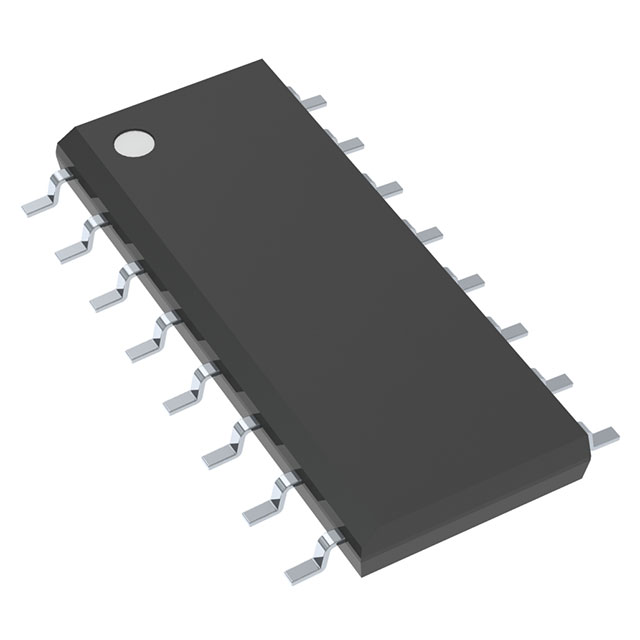
The CDCVF25081DRG4 is a high-performance PLL clock driver from Texas Instruments, designed to provide reliable and efficient clock distribution in various electronic systems. This device is housed in a 16-lead SOIC package, making it suitable for surface-mount applications. It operates within a supply voltage range of 3V to 3.6V and supports LVTTL input and output levels, ensuring compatibility with a wide range of digital circuits.
The CDCVF25081DRG4 features a phase-locked loop (PLL) with a bypass option, offering enhanced frequency stability and flexibility. It supports a maximum operating frequency of 200MHz, making it ideal for high-speed applications. The device has an input-to-output ratio of 2:8, allowing it to drive multiple loads efficiently. Additionally, it is REACH unaffected and RoHS3 compliant, ensuring environmental safety and regulatory compliance.
CDCVF25081DRG4 Features
- PLL with Bypass Option: The integrated PLL ensures precise clock generation and synchronization, while the bypass option allows for direct clock input when the PLL is not required.
- Wide Operating Voltage Range: The device operates reliably within a 3V to 3.6V supply voltage range, providing flexibility in power supply design.
- High-Speed Performance: With a maximum operating frequency of 200MHz, the CDCVF25081DRG4 is well-suited for high-speed digital systems.
- LVTTL Compatibility: The device supports LVTTL input and output levels, ensuring seamless integration with other digital circuits.
- Efficient Load Driving: The 2:8 input-to-output ratio allows the device to drive multiple loads efficiently, reducing the need for additional clock distribution components.
- Environmental Compliance: The device is REACH unaffected and RoHS3 compliant, meeting stringent environmental and regulatory standards.
- Surface-Mount Packaging: The 16-lead SOIC package is ideal for surface-mount applications, providing a compact and reliable solution for modern electronic designs.
CDCVF25081DRG4 Applications
The CDCVF25081DRG4 is ideal for a variety of applications where precise clock distribution and high-speed performance are critical. Some specific use cases include:
- High-Speed Digital Systems: The device's ability to operate at up to 200MHz makes it suitable for high-speed digital systems, such as FPGAs, ASICs, and microprocessors.
- Telecommunications: The reliable clock distribution and PLL capabilities make it an excellent choice for telecommunications equipment, where precise timing is essential.
- Data Centers: The efficient load driving and high-speed performance are beneficial for data center applications, ensuring reliable clock distribution across multiple devices.
- Consumer Electronics: The compact surface-mount package and wide operating voltage range make it suitable for consumer electronics, where space and power efficiency are critical.
Conclusion of CDCVF25081DRG4
The CDCVF25081DRG4 from Texas Instruments is a versatile and high-performance PLL clock driver, offering a range of features and benefits that make it an excellent choice for various electronic applications. Its wide operating voltage range, high-speed performance, and LVTTL compatibility ensure seamless integration into modern digital systems. The integrated PLL with a bypass option provides enhanced frequency stability and flexibility, while the efficient load driving capabilities reduce the need for additional components. With its compact surface-mount package and environmental compliance, the CDCVF25081DRG4 is a reliable and efficient solution for high-speed clock distribution in a variety of industries.
FAQ
Not available to buy online? Want the lower wholesale price? Please Send RFQ to get best price, we will respond immediately


.png?x-oss-process=image/format,webp/resize,h_32)


