
 German
 Japanese
 Portuguese
 Korea
Korea
 Mexico
 Dutch
Dutch


Texas Instruments
CDCVF25081PW

Why Choose Us?
Professional Platform
B2B & B2C purchasingDelivery at full speed
1-2 days deliveryWide variety
Original manufacturers365 days guarantee
Responsible quality
.png)


Tech Specifications
CDCVF25081PW Description
CDCVF25081PW Description
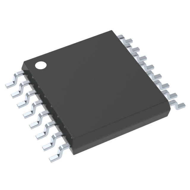
The CDCVF25081PW is a high-performance PLL clock driver from Texas Instruments, designed to provide reliable and efficient clock distribution in a variety of electronic systems. This device is housed in a 16-TSSOP package and is suitable for surface mount applications, making it ideal for compact and space-constrained designs. The CDCVF25081PW features a PLL with bypass capability, ensuring flexibility and adaptability in different operating conditions.
CDCVF25081PW Features
- PLL with Bypass Capability: The CDCVF25081PW incorporates a Phase-Locked Loop (PLL) that can be bypassed, offering enhanced flexibility and adaptability in various operating scenarios. This feature allows designers to optimize system performance and power consumption based on specific application requirements.
- Input and Output Compatibility: The device supports LVTTL input and output levels, ensuring compatibility with a wide range of digital systems. This compatibility simplifies integration and reduces the need for additional level-shifting components.
- Wide Supply Voltage Range: Operating within a supply voltage range of 3V to 3.6V, the CDCVF25081PW offers robust performance across a broad range of power supply conditions. This wide voltage range enhances the device's versatility and reliability in diverse applications.
- High Maximum Frequency: With a maximum operating frequency of 200MHz, the CDCVF25081PW is capable of supporting high-speed clock distribution, making it suitable for demanding applications that require precise timing and synchronization.
- Input to Output Ratio: The device features an input to output ratio of 2:8, allowing for efficient clock distribution and replication. This ratio is particularly beneficial in applications where multiple clock signals need to be generated from a single input source.
- Compliance and Standards: The CDCVF25081PW is REACH unaffected and ROHS3 compliant, ensuring that it meets stringent environmental and regulatory standards. Additionally, it has a moisture sensitivity level (MSL) of 1, indicating unlimited storage time and enhanced reliability in manufacturing processes.
- Packaging and Mounting: Housed in a tube package, the CDCVF25081PW is designed for surface mount applications, facilitating easy integration into modern printed circuit board (PCB) designs. This packaging option also ensures mechanical stability and durability during assembly and operation.
CDCVF25081PW Applications
The CDCVF25081PW is well-suited for a variety of applications that require precise clock distribution and synchronization. Some specific use cases include:
- Telecommunications: In telecommunication systems, the CDCVF25081PW can be used to distribute clock signals across various components, ensuring accurate timing and synchronization for data transmission and reception.
- Data Centers: For data center applications, the device can provide reliable clock distribution to multiple servers and networking equipment, maintaining optimal performance and minimizing latency.
- Industrial Control Systems: In industrial environments, the CDCVF25081PW can be employed to synchronize clock signals across different control modules and sensors, enhancing system reliability and accuracy.
- Consumer Electronics: The device is also suitable for consumer electronics, such as high-definition televisions and gaming consoles, where precise clock distribution is essential for high-quality video and audio processing.
Conclusion of CDCVF25081PW
The CDCVF25081PW from Texas Instruments is a versatile and high-performance PLL clock driver that offers a range of features and benefits for various electronic applications. Its wide supply voltage range, high maximum frequency, and flexible PLL with bypass capability make it an ideal choice for designers looking to achieve reliable clock distribution and synchronization. The device's compliance with environmental and regulatory standards, along with its surface mount packaging, ensures ease of integration and long-term reliability. Whether used in telecommunications, data centers, industrial control systems, or consumer electronics, the CDCVF25081PW provides a robust and efficient solution for precise clock management.
FAQ
| Quantity | Unit Price | Ext. Price |
|---|---|---|
| 1+ | $4.03040 | $4.03 |
| 10+ | $3.06328 | $30.63 |
| 90+ | $2.57117 | $231.41 |
| 98+ | $2.69280 | $263.89 |
| 180+ | $2.46909 | $444.44 |
Not available to buy online? Want the lower wholesale price? Please Send RFQ to get best price, we will respond immediately


.png?x-oss-process=image/format,webp/resize,h_32)


