
 German
 Japanese
 Portuguese
 Korea
Korea
 Mexico
 Dutch
Dutch


Texas Instruments
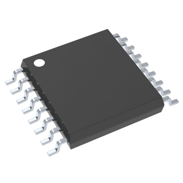
CDCVF25084PW

Why Choose Us?
Professional Platform
B2B & B2C purchasingDelivery at full speed
1-2 days deliveryWide variety
Original manufacturers365 days guarantee
Responsible quality
.png)


Tech Specifications
CDCVF25084PW Description
CDCVF25084PW Description
The CDCVF25084PW is a high-performance PLL Clock Multiplier designed by Texas Instruments, offering robust performance and flexibility for a wide range of clock management applications. This device is housed in a 16-TSSOP package, making it suitable for surface mount applications. It features a PLL with bypass capabilities, allowing for enhanced flexibility in clock generation and distribution.
CDCVF25084PW Features
- PLL with Bypass: The CDCVF25084PW includes a Phase-Locked Loop (PLL) with bypass functionality, enabling precise clock multiplication and distribution while maintaining signal integrity.
- Input and Output Compatibility: The device supports LVTTL input and output levels, ensuring compatibility with a broad range of digital systems.
- Wide Supply Voltage Range: Operating within a 3V to 3.6V supply voltage range, this IC is well-suited for various power supply configurations.
- High Frequency Capability: With a maximum frequency of 180MHz, the CDCVF25084PW is capable of handling high-speed clock signals, making it ideal for demanding applications.
- Input to Output Ratio: The 2:8 input to output ratio provides efficient clock multiplication, enhancing the device's versatility in clock management.
- Compliance and Sensitivity: The CDCVF25084PW is REACH unaffected and RoHS3 compliant, ensuring environmental and regulatory standards are met. Additionally, it has a Moisture Sensitivity Level (MSL) of 1, making it suitable for unlimited storage conditions.
- Package and Mounting: The 16-TSSOP package and surface mount mounting type offer ease of integration into compact and high-density designs.
CDCVF25084PW Applications
The CDCVF25084PW is ideal for applications requiring precise clock multiplication and distribution. Its high-frequency capability and wide supply voltage range make it suitable for:
- Telecommunications: Enhancing signal integrity and synchronization in high-speed communication systems.
- Data Processing: Providing reliable clock signals for data processing units and microprocessors.
- Networking: Ensuring accurate timing in network devices and switches.
- Consumer Electronics: Improving clock management in devices such as routers, modems, and set-top boxes.
Conclusion of CDCVF25084PW
The CDCVF25084PW from Texas Instruments stands out as a versatile and high-performance PLL Clock Multiplier. Its unique features, including the PLL with bypass, wide supply voltage range, and high-frequency capability, make it a reliable choice for clock management applications. The device's compliance with environmental and regulatory standards, along with its robust performance, ensures it meets the demands of modern electronics. Whether used in telecommunications, data processing, or consumer electronics, the CDCVF25084PW provides efficient and reliable clock multiplication, making it an essential component for any high-speed digital system.
FAQ
Not available to buy online? Want the lower wholesale price? Please Send RFQ to get best price, we will respond immediately


.png?x-oss-process=image/format,webp/resize,h_32)


