
 German
 Japanese
 Portuguese
 Korea
Korea
 Mexico
 Dutch
Dutch


Texas Instruments
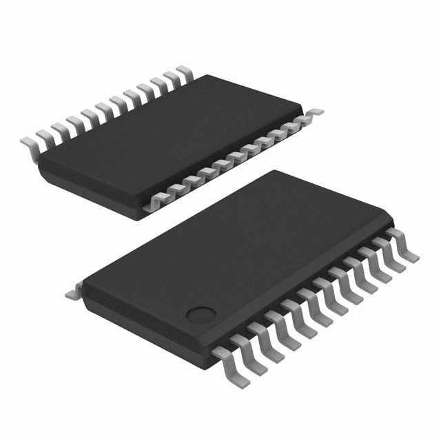
CDCVF2509PW

Why Choose Us?
Professional Platform
B2B & B2C purchasingDelivery at full speed
1-2 days deliveryWide variety
Original manufacturers365 days guarantee
Responsible quality
.png)


Tech Specifications
CDCVF2509PW Description
CDCVF2509PW Description
The CDCVF2509PW from Texas Instruments is a high-performance PLL-based clock driver designed for precision clock distribution in demanding electronic systems. Housed in a 24-pin TSSOP package, this device operates within a 3V to 3.6V supply range and supports LVTTL input/output levels, ensuring compatibility with modern digital circuits. With a maximum frequency of 175MHz, it delivers low-jitter, high-fidelity clock signals, making it ideal for applications requiring stable timing synchronization. The 2:10 input-to-output ratio enables efficient fan-out, while the integrated PLL with bypass capability provides flexibility in clock management.
CDCVF2509PW Features
- PLL with Bypass Mode: Allows seamless switching between PLL-synchronized and direct clock distribution for system redundancy.
- Low-Voltage Operation: Optimized for 3V–3.6V supplies, reducing power consumption in energy-sensitive designs.
- High Fan-Out Capability: 2:10 ratio minimizes the need for additional buffers, simplifying PCB layout.
- Wide Temperature Range: Operates reliably from 0°C to 85°C, suitable for industrial and commercial environments.
- LVTTL Compatibility: Ensures interoperability with standard logic families.
- RoHS3 & REACH Compliant: Meets stringent environmental regulations.
- 175MHz Max Frequency: Supports high-speed clocking for processors, FPGAs, and networking equipment.
CDCVF2509PW Applications
The CDCVF2509PW excels in systems requiring precise clock distribution, such as:
- Telecommunications: Synchronizing baseband processors and network switches.
- Data Centers: Clock tree management for servers and storage arrays.
- FPGA/ASIC Designs: Providing low-jitter reference clocks.
- Industrial Automation: Timing control for PLCs and motor drives.
- Test & Measurement Equipment: Ensuring accurate signal generation and capture.
Conclusion of CDCVF2509PW
The CDCVF2509PW stands out as a robust, flexible clock driver with PLL integration, low-voltage operation, and high fan-out capability. Its 175MHz performance and LVTTL compatibility make it a preferred choice for high-reliability applications in telecom, computing, and industrial systems. Texas Instruments’ commitment to quality ensures compliance with RoHS3 and REACH, further enhancing its suitability for modern electronic designs. For engineers seeking a balance of precision, efficiency, and scalability, this device delivers exceptional value.
FAQ
Not available to buy online? Want the lower wholesale price? Please Send RFQ to get best price, we will respond immediately


.png?x-oss-process=image/format,webp/resize,h_32)


