
 German
 Japanese
 Portuguese
 Korea
Korea
 Mexico
 Dutch
Dutch


Texas Instruments
CDCVF310PW

Why Choose Us?
Professional Platform
B2B & B2C purchasingDelivery at full speed
1-2 days deliveryWide variety
Original manufacturers365 days guarantee
Responsible quality
.png)


Tech Specifications
CDCVF310PW Description
CDCVF310PW Description
The CDCVF310PW is a high-performance clock fanout buffer designed for efficient clock signal distribution. Manufactured by Texas Instruments, this device falls under the category of Clock/Timing ICs and is ideal for applications requiring reliable and precise clock signal replication. The CDCVF310PW features a 1:10 input-to-output ratio, enabling it to distribute a single clock signal across ten output lines. This fanout buffer operates within a supply voltage range of 2.3V to 3.6V and supports LVTTL input and output levels, ensuring compatibility with a wide range of digital systems.
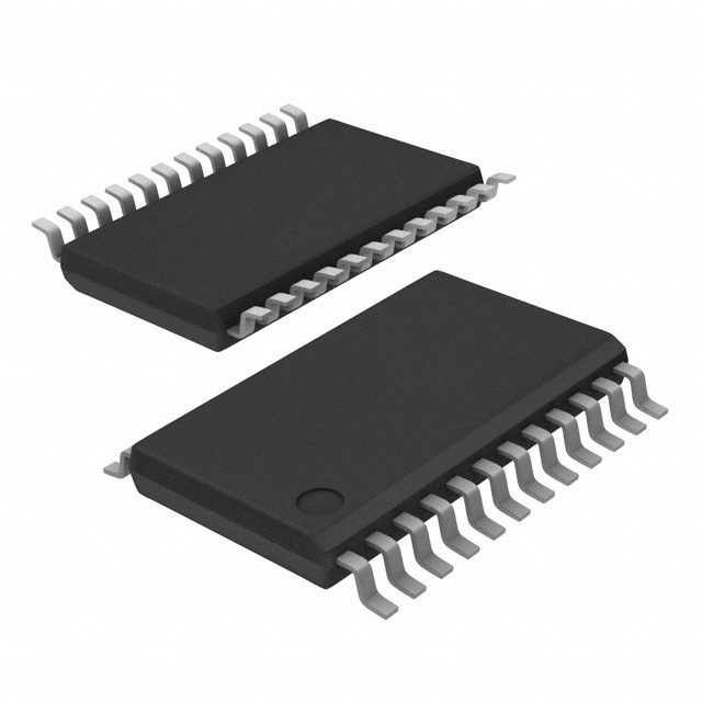
The CDCVF310PW is housed in a 24-TSSOP package, which is suitable for surface-mount applications, making it ideal for compact and high-density PCB designs. With a maximum operating frequency of 200 MHz, this device can handle high-speed clock signals with minimal propagation delay and jitter. The CDCVF310PW is REACH unaffected and RoHS3 compliant, adhering to stringent environmental regulations and ensuring safe usage in various industrial settings. Additionally, it has a moisture sensitivity level (MSL) of 1, indicating it is suitable for unlimited storage without special handling requirements.
CDCVF310PW Features
- High Fanout Capability: The 1:10 input-to-output ratio allows for efficient distribution of clock signals, reducing the need for multiple clock sources and simplifying circuit design.
- Wide Operating Voltage Range: The 2.3V to 3.6V supply voltage range ensures compatibility with various power supply configurations, enhancing the device's versatility.
- High-Speed Performance: With a maximum operating frequency of 200 MHz, the CDCVF310PW can handle high-speed clock signals, making it suitable for demanding applications such as high-frequency communication systems and advanced computing platforms.
- Surface-Mount Compatibility: The 24-TSSOP package is designed for surface-mount technology, enabling compact and high-density PCB layouts, which is crucial for modern electronic designs.
- Environmental Compliance: The REACH unaffected and RoHS3 compliant status ensures that the CDCVF310PW meets international environmental standards, making it suitable for global deployment.
- Low Moisture Sensitivity: The MSL 1 rating allows for unlimited storage and handling without the need for special precautions, simplifying logistics and reducing the risk of moisture-related damage.
CDCVF310PW Applications
The CDCVF310PW is well-suited for a variety of applications where reliable clock signal distribution is critical. These applications include:
- Telecommunications: In high-speed communication systems, the CDCVF310PW can distribute clock signals to multiple components, ensuring synchronized operation and minimizing signal degradation.
- Computing: In advanced computing platforms, such as servers and high-performance computing clusters, the CDCVF310PW can distribute clock signals to various processing units, maintaining precise timing and improving overall system performance.
- Consumer Electronics: In devices such as smartphones, tablets, and smart TVs, the CDCVF310PW can distribute clock signals to multiple subsystems, ensuring synchronized operation and enhancing user experience.
- Industrial Control Systems: In industrial automation and control systems, the CDCVF310PW can distribute clock signals to various sensors and actuators, ensuring precise timing and improving system reliability.
Conclusion of CDCVF310PW
The CDCVF310PW from Texas Instruments is a robust and versatile clock fanout buffer that offers high-performance clock signal distribution. Its 1:10 fanout capability, wide operating voltage range, and high-speed performance make it an ideal choice for a variety of applications, from telecommunications to consumer electronics. The surface-mount compatibility, environmental compliance, and low moisture sensitivity further enhance its appeal for modern electronic designs. By providing reliable and precise clock signal distribution, the CDCVF310PW ensures synchronized operation and improved system performance, making it a valuable component in the electronics industry.
FAQ
Not available to buy online? Want the lower wholesale price? Please Send RFQ to get best price, we will respond immediately


.png?x-oss-process=image/format,webp/resize,h_32)


