
 German
 Japanese
 Portuguese
 Korea
Korea
 Mexico
 Dutch
Dutch


Texas Instruments
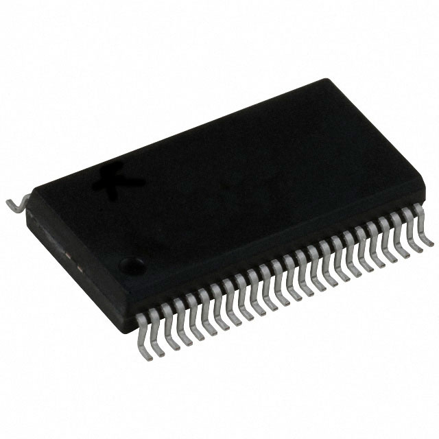
CDCVF857DGG

Why Choose Us?
Professional Platform
B2B & B2C purchasingDelivery at full speed
1-2 days deliveryWide variety
Original manufacturers365 days guarantee
Responsible quality
.png)


Tech Specifications
CDCVF857DGG Description
CDCVF857DGG Description
The CDCVF857DGG is a high-performance PLL clock driver designed by Texas Instruments, a leading manufacturer in the electronics industry. This IC is part of the Clock/Timing ICs category and is housed in a 48-TSSOP package, making it suitable for surface mount applications. The CDCVF857DGG features a wide supply voltage range of 2.3V to 2.7V, ensuring compatibility with various power supply configurations. It supports a maximum operating frequency of 220MHz, making it ideal for high-speed clock distribution and synchronization in complex electronic systems.
The CDCVF857DGG incorporates a Phase-Locked Loop (PLL) with bypass functionality, providing flexibility in clock generation and distribution. This feature allows for precise control over clock signals, reducing jitter and improving overall system performance. The device also supports differential input and output, which enhances signal integrity and reduces electromagnetic interference (EMI) in high-speed applications.
CDCVF857DGG Features
- PLL with Bypass: The CDCVF857DGG features an integrated PLL with bypass capabilities, allowing for flexible clock generation and distribution.
- Wide Supply Voltage Range: Operates within a 2.3V to 2.7V supply voltage range, ensuring compatibility with various power supply configurations.
- High-Speed Performance: Supports a maximum operating frequency of 220MHz, making it suitable for high-speed clock distribution.
- Differential I/O: Supports differential input and output, enhancing signal integrity and reducing EMI.
- Compliance and Reliability: The CDCVF857DGG is REACH unaffected and RoHS3 compliant, ensuring environmental and safety standards are met. It also has a Moisture Sensitivity Level (MSL) of 2 (1 Year), making it suitable for a variety of manufacturing environments.
- Packaging: Available in a Tube package, facilitating easy handling and integration into surface mount designs.
CDCVF857DGG Applications
The CDCVF857DGG is ideal for a variety of applications requiring high-speed clock distribution and synchronization. Some specific use cases include:
- Telecommunications: Used in base stations and communication equipment where precise clock synchronization is critical.
- Networking: Ideal for switches, routers, and other networking devices that require high-speed clock distribution.
- Data Centers: Used in servers and storage systems to ensure reliable and synchronized clock signals.
- Industrial Automation: Suitable for industrial control systems where high-speed clock distribution is necessary for real-time processing and control.
Conclusion of CDCVF857DGG
The CDCVF857DGG from Texas Instruments is a robust PLL clock driver designed to meet the demands of high-speed clock distribution in various electronic systems. Its wide supply voltage range, high operating frequency, and differential I/O capabilities make it a versatile and reliable choice for applications in telecommunications, networking, data centers, and industrial automation. The inclusion of a PLL with bypass functionality and compliance with environmental and safety standards further enhance its appeal. The CDCVF857DGG is an excellent choice for engineers and designers looking for a high-performance clock driver that can improve system performance and reliability.
FAQ
Not available to buy online? Want the lower wholesale price? Please Send RFQ to get best price, we will respond immediately


.png?x-oss-process=image/format,webp/resize,h_32)


