
 German
 Japanese
 Portuguese
 Korea
Korea
 Mexico
 Dutch
Dutch


Texas Instruments
CDCVF857RHATG4

Why Choose Us?
Professional Platform
B2B & B2C purchasingDelivery at full speed
1-2 days deliveryWide variety
Original manufacturers365 days guarantee
Responsible quality
.png)


Tech Specifications
CDCVF857RHATG4 Description
CDCVF857RHATG4 Description
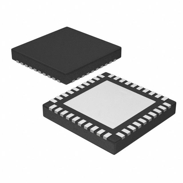
The CDCVF857RHATG4 is a high-performance PLL clock driver from Texas Instruments, designed to deliver reliable and efficient clock distribution in a variety of electronic systems. This IC is housed in a 40VQFN package, making it suitable for surface-mount applications. It operates within a supply voltage range of 2.3V to 2.7V and supports a maximum frequency of 220MHz, ensuring compatibility with a wide range of modern digital circuits.
CDCVF857RHATG4 Features
- PLL with Bypass Capability: The CDCVF857RHATG4 features an integrated Phase-Locked Loop (PLL) with bypass functionality, allowing for flexible clock management and optimization of performance based on specific application requirements.
- Differential I/O: This IC supports differential input and output, which enhances signal integrity and reduces electromagnetic interference (EMI), making it ideal for high-speed and high-reliability applications.
- 2:11 Input to Output Ratio: The CDCVF857RHATG4 offers a 2:11 input-to-output ratio, providing efficient clock multiplication and distribution, which is essential for systems requiring multiple clock frequencies.
- Compliance and Reliability: The IC is REACH unaffected and RoHS3 compliant, ensuring it meets stringent environmental and safety standards. Additionally, it has a Moisture Sensitivity Level (MSL) of 3 (168 hours), making it suitable for various manufacturing environments.
- Single Circuit Design: With a single circuit design, the CDCVF857RHATG4 simplifies integration into complex systems, reducing the overall footprint and complexity of the design.
- Surface Mount Technology: The surface-mount packaging of the CDCVF857RHATG4 facilitates automated assembly processes, enhancing manufacturing efficiency and reliability.
CDCVF857RHATG4 Applications
The CDCVF857RHATG4 is well-suited for a variety of applications that require precise clock distribution and management. Its high-frequency capability and differential signaling make it ideal for:
- Telecommunications: Use in base stations, switches, and routers where high-speed data transmission and signal integrity are critical.
- Networking: Ideal for Ethernet switches, routers, and other networking equipment that require reliable clock synchronization.
- Data Centers: Suitable for server and storage systems that demand high-performance clock distribution to ensure data integrity and system reliability.
- Industrial Automation: Applicable in industrial control systems where precise timing and synchronization are essential for process control and automation.
- Consumer Electronics: Useful in high-end consumer devices such as gaming consoles, smart TVs, and advanced set-top boxes where high-speed clock distribution is necessary.
Conclusion of CDCVF857RHATG4
The CDCVF857RHATG4 from Texas Instruments stands out as a robust and versatile PLL clock driver, offering a combination of high performance, flexibility, and compliance with industry standards. Its differential I/O, PLL with bypass, and wide operating frequency range make it a reliable choice for a variety of demanding applications. Whether in telecommunications, networking, data centers, industrial automation, or consumer electronics, the CDCVF857RHATG4 provides the precision and reliability needed to ensure optimal system performance.
FAQ
Not available to buy online? Want the lower wholesale price? Please Send RFQ to get best price, we will respond immediately


.png?x-oss-process=image/format,webp/resize,h_32)


